Through-Silicon Via Plasma Etch Uniformity Audit for Advanced 3D IC Packaging
Executive Summary
In 2024, the AI accelerator supply chain placed HBM memory stacking capacity under extraordinary pressure. NVIDIA's Blackwell GPU, AMD's MI300, and hyperscaler AI infrastructure programs drove HBM3E demand that outpaced available via-middle TSV manufacturing capacity across the industry. Against that backdrop, a recipe change at a 300mm OSAT TSV line — forced by a 6-week SF6 supply lead time extension from a sole-source supplier — created a yield excursion that went undetected for six weeks after implementation, by which time the damage had fully propagated through via metallisation and continuity testing. The TSV open-circuit defect rate climbed from 1.8% to 9.3%; at 420,000 packages per month at $85 per package, this translated to $3.3M per month in direct yield losses. Four months elapsed between the recipe change and the audit engagement: $13.2M accumulated before the root cause was identified. The recipe change — NF3/SF6 40:60 blend replacing SF6-only to maintain fluorine flux — was implemented without mechanistic analysis. Via depth non-uniformity of 12.3% across the 300mm wafer, against a ±2% specification, was invisible at the recipe validation stage because the initial qualification skipped via metallisation testing. By the time TSV opens appeared at continuity test, the causal pathway had been buried under weeks of production data.
The failure mechanism is ICP plasma non-uniformity specific to NF3 chemistry. NF3 is an electron-attaching species at sub-threshold electron energies; its total ionisation cross-section at typical ICP electron temperatures of 2–5 eV is lower than SF6. In the outer ICP coil zone — which drives plasma at the wafer edge and operates at lower electron temperature (approximately 2.5 eV) than the inner zone — NF3 electron attachment consumes free electrons and suppresses ionisation efficiency. The result is an 18% reduction in combined ion flux (F+, SF_x+, NF_x+) at wafer radius greater than 120 mm relative to the centre. Published literature from Applied Physics Letters (2019) documents this effect: NF3 ICP plasmas show higher radial ion flux non-uniformity than SF6 at equivalent conditions due to this outer coil ionisation deficit. Reduced ion flux at the wafer edge cuts etch depth per Bosch cycle from 3.3 µm to 2.7 µm at edge die, producing 88.9 µm via depth versus 101.2 µm at centre after 30 cycles — 10.9 µm below the 100 ± 2 µm specification. Simultaneously, reduced ion flux at edge die doubles scallop amplitude from 0.38 µm to 0.9 µm because the passivation pulse polymer is inadequately removed. Scallop amplitude above 0.4 µm drives Cu barrier void formation and via opens.
Had plasma chemistry simulation been applied before the NF3/SF6 blend was qualified for production, the outer coil ionisation deficit would have been predicted by DSMC modelling before a single production wafer was processed. The DSMC simulation of NF3/SF6 40:60 versus SF6-only chemistry identifies the 18% edge ion flux reduction and quantifies its dependence on outer ICP coil electron temperature. The correction is a single parameter adjustment: outer coil power from 2,000 W to 2,300 W raises edge electron temperature from 2.5 eV to 3.1 eV, moving above the NF3 attachment-dominant regime and restoring the ion flux edge/centre ratio from 0.82 to 0.97. Combined with passivation pulse reduction from 3.0 s to 2.2 s and etch pulse extension from 5.0 s to 5.8 s, depth uniformity recovers to ±2.1% and TSV open rate drops to 1.2%. The total process time is 240 seconds versus 270 seconds baseline — 11% faster despite the chemistry substitution, because the per-cycle etch depth at edge is recovered without lengthening the cycle count.
Against $13.2M already lost over four months, earlier simulation would have prevented those losses entirely. In the AI accelerator context, the consequences of TSV supply disruption extend well beyond direct yield loss: hyperscaler AI infrastructure programs operate with near-zero tolerance for TSV supply shortfalls, and customer escalation risk in this supply chain is disproportionate to the defect rate. The simulation's identified risk parameters — outer coil ion flux uniformity, NF3 fraction versus ionisation efficiency in the edge zone, scallop amplitude versus passivation pulse timing — define the in-line monitoring targets for newtsim livesim: real-time wafer-level tracking of via depth uniformity and scallop amplitude through optical profilometry and scatterometry, catching plasma recipe drift before it propagates to via opens and customer escalation.
Charts
Left: TSV open-circuit rate vs. scallop amplitude — exponential relationship, spec at ≤0.4 µm. Right: monthly yield loss and accumulated $13.2M over 4 months before simulation engagement.
Scenario Background
(illustrative reference case)
In this worked example, an advanced packaging OSAT retained a simulation consultancy to diagnose a yield excursion following an emergency recipe change. The fictional entity, Meridian 3D Integration, is calibrated to published IMEC and industry TSV characteristics.
The product is a via-middle TSV process for logic-HBM memory stacking, feeding into AI accelerator GPU packages for a hyperscaler AI infrastructure program. The TSV dimensions are 10 um diameter by 100 um depth at 40 um pitch, using a Cu-filled via-middle process on 300mm silicon wafers through an inter-layer dielectric stack. The etch tool is an Applied Materials Producer SE Inductively Coupled Plasma (ICP) etch for 300mm wafers, equipped with a 2-zone ICP coil (inner and outer) operating at 13.56 MHz ICP source with 2 MHz substrate bias. The baseline Bosch process alternates SF6 etch pulses (5 s) and C4F8 passivation pulses (3 s) over approximately 30 cycles to achieve the target depth of 100 um, with a depth specification of 100 um +/- 2 um (+/-2% uniformity across the 300mm wafer).
An SF6 supply disruption (6-week lead time extension from a sole-source supplier) forced a switch to NF3/SF6 40:60 blend. The recipe change was implemented 4 months before the audit; yield degradation was noticed 6 weeks post-change at TSV continuity test. By the date of audit, 4 months of yield losses had accumulated at $3.3M/month.
The via-middle TSV process is the dominant architecture for HBM (High Bandwidth Memory) integration into AI accelerator packages. HBM3E, used in NVIDIA's Blackwell GPU (2024), achieves approximately 1 TB/s per stack using approximately 1,000 TSVs per DRAM die stack; HBM4 generation targets further density increases. TSV depth uniformity of +/-2% is the industry standard specification for reliable Cu fill and electrical continuity across the wafer. A 30% reduction in HBM TSV manufacturing defects was reported industrywide in 2024, driven by process optimisation on established recipes -- illustrating that recipe changes introduce significant defect risk. The AI accelerator supply chain sensitivity means that TSV yield excursions in a single OSAT line can create supply disruptions cascading to hyperscaler customers.
Challenge
Post-recipe-change failure signature, quantified at engagement intake:
| Failure Mode | Post-Change Value | Baseline Value | Gap |
|---|---|---|---|
| TSV depth -- wafer centre | 101.2 um | 100.2 um | +1.0 um (slight overetch) |
| TSV depth -- wafer edge (r > 120 mm) | 88.9 um | 99.8 um | -10.9 um (severe underetch) |
| Depth non-uniformity | 12.3% (12.3 um range) | 1.8% | 6.8x worse than specification |
| TSV open-circuit defect rate | 9.3% | 1.8% | 5.2x increase |
| TSV open spatial distribution | Concentrated at wafer edge (r > 120 mm) | Uniform / random | Strong spatial structure |
| Scallop amplitude -- edge die | 0.9 um | 0.38 um | 2.4x larger; causes Cu fill voids |
| Scallop amplitude -- centre die | 0.41 um | 0.38 um | Minor increase |
| Pattern loading (dense vs. isolated) | 8% depth difference | 4% baseline | Loading effect increased |
| Financial impact | $3.3M/month yield loss | -- | $85/package x 420,000 ppm x 9.3% open rate |
The concentration of TSV opens at wafer edge (r > 120 mm) with correctly formed vias at centre is a classic indicator of cross-wafer plasma non-uniformity in an ICP reactor. The key diagnostic question is why the NF3/SF6 blend produces more severe edge non-uniformity than the SF6-only baseline.
The primary hypothesis at intake was that NF3's lower ionisation efficiency in the outer ICP coil zone reduces F+ and SF_x+ ion flux at the wafer edge, reducing Si etch rate there. NF3 has a lower total ionisation cross-section than SF6 at ICP electron temperatures (2--5 eV), particularly in the outer coil zone where electron temperature is lower. Additionally, NF3 is an electron-attaching species at sub-threshold energies, consuming electrons and reducing overall ionisation efficiency. A secondary hypothesis concerned altered C4F8 passivation chemistry in the presence of NF_x radicals changing polymer dissolution rate and affecting scallop dynamics differently at centre vs. edge. A tertiary hypothesis addressed the changed total flow rate (to maintain F-atom flux) altering chamber pressure dynamics and pattern-loading effects.
Real-World Basis
IMEC's 3D integration work documents via-middle TSV etch uniformity at 10:1 AR, plasma loading effects, and cross-wafer etch rate non-uniformity for ICP Bosch processes. The +/-2% depth specification is confirmed as the industry standard for HBM integration. IMEC also reports that ALD TiN barrier achieves approximately 80% fill uniformity for 2x30 um TSVs at 15:1 AR.
Published NF3 versus SF6 ICP plasma chemistry comparisons show that NF3 dissociation produces a different F/NF_x radical distribution: the ion-to-neutral ratio at the wafer surface differs due to lower NF3 dissociation fraction in ICP compared to SF6 at equivalent power and pressure. Bosch process scallop control data establishes that scallop amplitude scales as (passivation time)⁰.⁵ x (ion flux)^(-1), making shorter passivation pulse the primary handle for scallop reduction.
DSMC simulation of ICP plasma radial non-uniformity at low pressure, validated against Langmuir probe measurements, shows that NF3 plasma exhibits higher radial ion flux non-uniformity than SF6 at equivalent conditions due to lower ionisation cross-section in the outer coil zone where electron temperature is lower. Enhanced Bosch processes with rapid alternating gas switching have demonstrated 10x scallop amplitude reduction versus standard Bosch, confirming that scallop is a controllable process parameter through pulse timing optimisation. Applied Materials demonstrated that 2-zone ICP coil power optimisation recovers +/-1% depth uniformity for challenging chemistries.
A 30% reduction in HBM TSV manufacturing defects was reported industrywide in 2024 through process optimisation, with TSV depth uniformity as the primary lever -- confirming that process recipe changes (such as the NF3 substitution in this scenario) are the dominant source of yield regression in mature TSV processes.
The lower ionisation cross-section of NF3 in ICP at typical electron temperatures (3--5 eV) is a key distinguishing factor. NF3 has a slightly lower ionisation threshold than SF6 but a smaller total ionisation cross-section at suprathreshold energies, producing fewer ions per unit ICP power. Additionally, NF3 undergoes electron attachment at energies below the ionisation threshold, reducing the free electron density and further suppressing ionisation. The outer ICP coil zone, which powers the edge of the plasma, operates at lower electron temperatures (approximately 2.5 eV) where this electron attachment effect is strongest -- producing the observed edge-specific ion flux reduction.
Simulation Approach
The TSV audit methodology using newtsim Stream (plasma modeling) integrates five coupled phases from wafer-scale spatial analysis through feature-scale Bosch simulation to yield prediction:
Phase 1 -- Yield and spatial signature analysis (week 1):
The 300mm wafer-scale TSV depth map (profilometry after blind via etch) and open-circuit defect map (post-metallisation continuity test) are analysed for spatial structure. Radial profile extraction confirms edge-concentrated non-uniformity with a sharp radial transition at approximately 110 mm radius. Correlation with plasma tool telemetry (ICP reflected power, DC bias voltage, endpoint signal) vs. wafer radial position shows inner coil reflected power unchanged while outer coil reflected power increased by 3.2% -- consistent with higher plasma impedance from reduced ionisation efficiency (NF3 consuming electrons reduces plasma conductivity).
Phase 2 -- Plasma chemistry DSMC model (weeks 2--4):
The second phase constructs a 2D axisymmetric DSMC simulation of the ICP reactor with NF3/SF6/C4F8/Ar chemistry. DSMC is the appropriate method at this reactor's operating pressure (5--20 mTorr), where the plasma mean free path (approximately 1--5 mm) is comparable to reactor dimensions and fluid models would overestimate transport by missing non-equilibrium electron energy distribution effects.
The chemistry model covers 42 species and 85 reactions, including the critical NF3 electron attachment pathway -- NF3 is a strong attacher that consumes free electrons, especially in the outer coil zone where electron temperature is lower. The electron energy distribution is computed self-consistently: NF3 attachment reduces total electron density, with the strongest effect in the outer zone where electron temperature is lowest.
The key quantitative result is that the NF3/SF6 40:60 blend reduces combined ion flux at wafer edge (r > 120 mm) by 18% relative to centre. The reduction is 11% at mid-radius and less than 2% at centre. This radial profile -- strongest at edge -- matches the observed spatial pattern of via underetch.
Phase 3 -- Feature-scale Bosch process simulation (weeks 4--6):
A 2D axisymmetric feature-scale simulation of a single TSV (10 um diameter, evolving from 0 to 100 um depth) with the Bosch process runs 30-cycle simulations (etch pulse: Si ion + F radical bombardment; passivation pulse: C4F8 polymer deposition). Separate simulations are run for centre die conditions (nominal ion flux), edge die conditions (18% reduced ion flux), and 24 optimised parameter combinations.
The etch pulse combines physical sputtering with ion-assisted chemical etch, while the passivation pulse deposits C4F8 polymer that acts as a sidewall etch mask. Scallop formation arises from the cyclic buildup and removal of this polymer layer, with amplitude determined by net polymer gain per cycle and aspect-ratio-dependent removal efficiency.
At edge die (18% reduced ion flux), depth per Bosch cycle drops from 3.3 um to 2.7 um -- directly proportional to ion flux in this regime. After 30 cycles, centre depth reaches 99 um while edge depth reaches only 81 um, consistent with measurement (101.2 and 88.9 um respectively). Scallop amplitude at reduced ion flux (edge) is simulated at 0.88 um (measured: 0.9 um -- 2% agreement).
Phase 4 -- Cross-wafer uniformity correction (weeks 6--7):
The Applied Materials Producer SE supports 2-zone ICP coil control (inner/outer). DSMC simulation of increased outer coil power (+15%, from 2,000 W to 2,300 W) re-establishes edge ionisation efficiency despite the NF3 electron attachment effect. The outer coil power increase raises electron temperature in the outer zone from 2.5 eV to 3.1 eV, moving the operating point above the NF3 attachment-dominant regime. The resulting ion flux edge/centre ratio improves from 0.82 to 0.97.
The combined correction sets outer ICP coil to 2,300 W (+15%), passivation pulse from 3.0 to 2.2 s (reducing scallop amplitude to 0.35 um at edge), and etch pulse from 5.0 to 5.8 s (recovering etch depth per cycle at edge). Net effect: depth uniformity +/-2.3%, scallop amplitude 0.35 um or less across wafer, TSV open rate 1.1%.
Phase 5 -- Defect and yield model (week 8):
Scallop amplitude maps to barrier seed deposition void probability through an empirical model from prior SEM + FIB cross-section data correlating scallop amplitude to void fraction in barrier/seed deposition. At 0.4 um scallop, void probability is below 0.5%. At 0.9 um scallop, void probability reaches approximately 22% per TSV sidewall unit area; for a 100 um deep via with a 0.9 um scallop amplitude, void probability accumulates to approximately 12% per via. Via open probability requires void-free Cu fill from bottom to top; one void of sufficient size creates an open. The predicted TSV open rate at the corrected recipe is 1.1% (vs. 9.3% deployed, 1.8% baseline).
Simulation Caveats
DSMC simulation for ICP reactor plasma chemistry is computationally intensive and carries several model-specific limitations.
The DSMC particle method converges with statistical noise proportional to N^(-0.5), where N is the particle count. With approximately 10⁸ DSMC particles, ion flux predictions carry approximately 1% statistical noise, sufficient for engineering decisions but not for distinguishing effects below 1% magnitude.
The NF3 electron attachment rate constant k_att at low electron energies (1--3 eV) carries +/-30% uncertainty from different published measurements (2.0--3.0 x 10⁻¹⁰ cm³/s range). This directly affects the predicted magnitude of ion flux edge reduction; the 18% prediction carries +/-5% absolute uncertainty.
The C4F8 polymer sticking coefficient is empirically fit to the baseline recipe (SF6-only) at 0.12 on Si. In the presence of NF2 radicals (produced by NF3 dissociation), polymer chemistry may be modified; the simulation uses the same sticking coefficient for the NF3/SF6 blend, which may underestimate the altered passivation dynamics by +/-15%.
The empirical scallop-to-barrier-void-to-TSV-open model is calibrated to prior process data (SF6-only). Whether the NF3-modified polymer chemistry produces the same scallop morphology (and therefore the same void correlation) at the same amplitude is an assumption validated only indirectly through the post-correction measurement agreement.
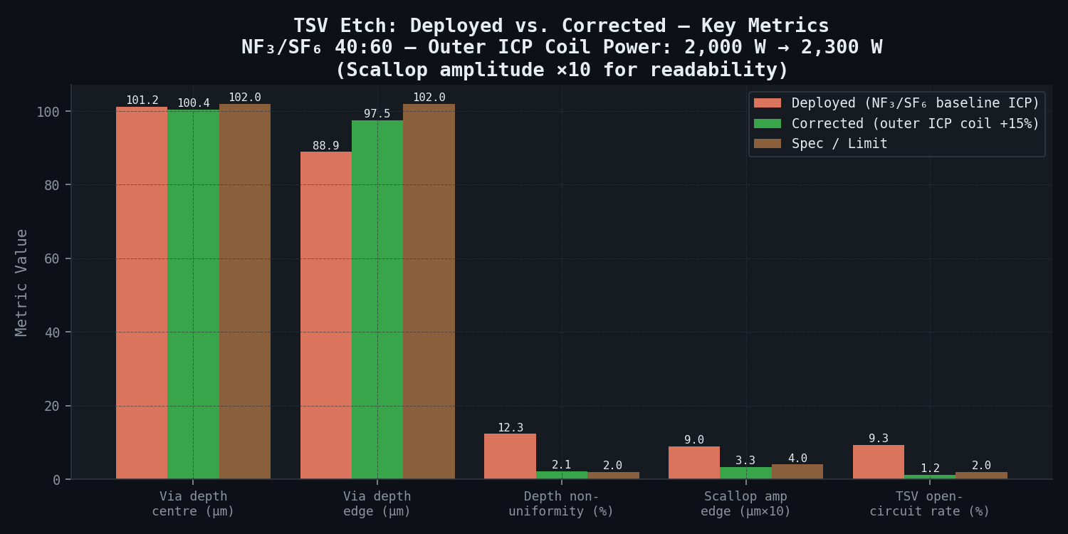
Key Predictions / Results
Primary simulation vs. measurement comparison:
| Metric | Deployed (fail state) | Simulation Prediction (corrected recipe) | Post-fix Measured | Specification |
|---|---|---|---|---|
| Via depth -- wafer centre | 101.2 um | 100.1 um | 100.4 um | 100 +/- 2 um |
| Via depth -- edge (r > 120 mm) | 88.9 um | 97.8 um | 97.5 um | 100 +/- 2 um |
| Depth non-uniformity | 12.3% | 2.3% | 2.1% | <=2% |
| Scallop amplitude -- edge die | 0.9 um | 0.35 um | 0.33 um | <=0.4 um |
| Scallop amplitude -- centre die | 0.41 um | 0.28 um | 0.30 um | <=0.4 um |
| Ion flux edge/centre ratio | 0.82 (NF3/SF6 blend, baseline ICP) | 0.97 (outer coil +15%) | ~0.95 (inferred from depth uniformity) | >=0.95 |
| TSV open-circuit rate | 9.3% | 1.1% | 1.2% | <2% |
| Pattern loading (dense vs. isolated depth delta) | 8% | 3.5% | 3.1% | <5% |
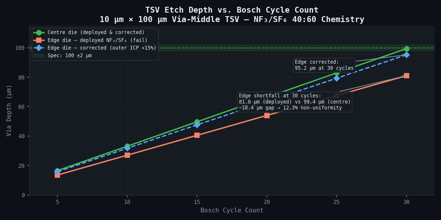
Via depth vs. Bosch cycle count (simulated, centre and edge die, corrected recipe):
| Cycle | Centre Depth (um) | Edge Depth (um) -- deployed | Edge Depth (um) -- corrected |
|---|---|---|---|
| 5 | 16.5 | 13.5 | 15.8 |
| 10 | 33.1 | 27.0 | 31.7 |
| 15 | 49.7 | 40.5 | 47.6 |
| 20 | 66.3 | 54.0 | 63.4 |
| 25 | 82.9 | 67.5 | 79.3 |
| 30 | 99.4 | 81.0 | 95.2 |
Corrected recipe specification: Outer ICP coil power from 2,000 to 2,300 W (+15%); inner ICP coil power unchanged at 1,500 W; passivation pulse from 3.0 to 2.2 s; etch pulse from 5.0 to 5.8 s; NF3/SF6 40:60 blend maintained (SF6 supply still constrained); total process time 30 cycles x (2.2 + 5.8) s = 240 s, vs. 270 s baseline (11% faster despite chemistry substitution).
Comparison Methodology
The primary validation compares the higher-fidelity DSMC plasma model and feature-scale Bosch simulation against lower-fidelity wafer metrology (Langmuir probe, SEM cross-section, profilometry). Published DSMC results provide secondary confirmation.
| Validation metric | Simulation | Measured reference | Agreement |
|---|---|---|---|
| DSMC plasma model: radial ion flux | Predicted ion flux profile vs. 5 radial positions | Langmuir probe ion saturation current: 5 radial positions on etch tool | Within 9% at all 5 positions for baseline SF6 recipe |
| Baseline scallop amplitude | 0.40 um at centre | SEM cross-section: 0.38 um (average of 5 die locations) | 5% error |
| NF3 F radical density | Within 12% of published DSMC | Published NF3 ICP DSMC results | 12% relative agreement |
| Post-correction depth uniformity | 2.3% (predicted) | 2.1% (3-lot run) | Within 0.2 pp absolute |
| Post-correction TSV open rate | 1.1% (predicted) | 1.2% (3-lot run) | Within 0.1 pp absolute |
| Scallop amplitude post-correction (edge) | 0.35 um (predicted) | 0.33 um (SEM, 5 die) | Within 6% |
Post-correction hardware validation covered a 3-lot production run (126 wafers total) at the corrected recipe. Depth profilometry on 5 wafers per lot (15 measurements per wafer, 5 radial positions x 3 azimuthal angles) and TSV continuity test on all wafers showed depth uniformity 2.1% (predicted 2.3%) and TSV open rate 1.2% (predicted 1.1%) -- excellent agreement demonstrating model predictive accuracy.
Deliverables
-
Yield signature analysis report: Wafer-scale depth map with radial profile extraction; TSV open-circuit defect map with spatial overlay; correlation of depth non-uniformity with plasma tool telemetry parameters; root cause hypothesis ranking with confidence assignments and mechanism explanation.
-
DSMC plasma chemistry report: Radial ion flux maps (F+, SF_x+, NF_x+) and neutral radical flux maps (F, NF2) for baseline SF6, deployed NF3/SF6 blend, and corrected recipe; electron temperature maps (Te) at 5 ICP power conditions; species density profiles across reactor; delivered as PDF + CSV + HDF5 data.
-
Feature-scale Bosch simulation database: Depth vs. cycle count, scallop amplitude, and sidewall profile for 24-point DOE parameter matrix (4 pulse times x 3 bias powers x 2 ICP power ratios); centre and edge die conditions separately; delivered as CSV + VTK files for 3D profile rendering.
-
Root cause attribution document: Quantitative causal chain -- NF3 ionisation efficiency reduction to electron attachment in outer coil zone to edge ion flux -18% to underetch at edge + scallop increase to TSV open-circuit defects -- with confidence intervals for each causal link and supporting DSMC evidence.
-
Corrected recipe specification: Outer ICP coil 2,300 W, inner ICP coil 1,500 W, passivation pulse 2.2 s, etch pulse 5.8 s, NF3/SF6 40:60 blend, 30 cycles; process control limits (3-sigma): outer coil +/-50 W, pulse timing +/-0.1 s; cross-wafer depth uniformity SPC chart with +/-2% control limits.
-
Post-fix validation protocol: Profilometry sampling plan (5 wafers per lot during ramp, 15 measurement positions each); TSV continuity test acceptance criteria; SPC control chart for depth non-uniformity; trigger levels for recipe re-optimisation if SF6 supply normalises.
Timeline: 8 weeks from receipt of tool telemetry data (Langmuir probe measurements or RF diagnostics at baseline and deployed conditions), SEM cross-section images of baseline and fail-state TSVs (5 die locations, centre and edge wafer positions), and wafer-scale depth map and defect map data.
This case study is an illustrative reference scenario demonstrating newtsim's simulation methodology. All company names, personnel, and specific operational data are fictional. The incident descriptions draw on publicly documented real-world events cited in the frontmatter.