SiC Epitaxial Layer Threading Screw Dislocation Root Cause Analysis for Power MOSFET Yield
Executive Summary
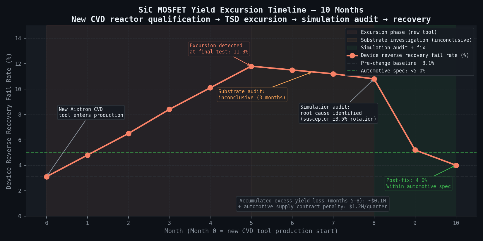
In the 2023–2025 period, the SiC power semiconductor supply chain operated under acute stress. Wolfspeed and STMicroelectronics carried multi-year order backlogs for automotive-grade 4H-SiC MOSFETs as EV traction inverter demand from OEMs including Tesla, BYD, BMW, and GM outpaced manufacturing capacity. In that environment, a step-change yield excursion on a 150mm 4H-SiC epitaxy line — device reverse recovery failure rate rising from 3.1% to 11.8% over five months following a new CVD reactor qualification — was not merely a process engineering problem. At 180,000 devices per month at $12 per device, the 8.7 percentage-point yield increase represented $187,000 per month in direct losses; accumulated over five months before the audit was commissioned, the total exceeded $935,000. Automotive OEM supply contract penalty exposure added $1.2M per quarter. What made the situation more damaging was the three-month substrate supplier investigation that preceded the audit: the failure was systematically blamed on incoming wafer quality when the root cause was entirely within the fab's own equipment.
The spatial pattern of failures told the story the substrate audit could not. KOH etch pit density maps across 15 production wafers showed TSD density of 380 cm⁻² concentrated in a 15–35 mm annular ring from the wafer edge — 4.2x above the 90 cm⁻² automotive specification — while the wafer centre remained at 95 cm⁻², near-nominal. Substrate incoming TSD density showed no correlation with lot fail rate (Pearson r = 0.12, p = 0.41). The annular pattern is the characteristic spatial signature of centrifugal gas redistribution during susceptor rotation speed transients in hot-wall CVD reactors: tool telemetry from the new Aixtron CVD system showed rotation speed variation of ±3.5% versus ±0.5% for the incumbent Nuflare tool — a 7x degradation in rotational stability that had passed equipment vendor qualification without triggering a process alarm. The mechanism: at ±3.5% speed variation, centrifugal forces during transients preferentially redistribute higher-molecular-weight Si-bearing species toward the wafer edge, driving Si/C ratio from the optimal 0.88–0.95 window into Si-rich excursions above 1.05. Published work establishes that Si-rich conditions during 4H-SiC step-flow growth at 1600°C destabilise the BPD-to-TED conversion pathway — the benign, sessile threading edge dislocation pathway — in favour of BPD-to-TSD conversion. TSDs propagate vertically through the 10 µm epitaxial layer to the device-active region, where they act as local electric field concentrators. Honda and Denso documented SiC MOSFET body diode failure at 0.75x rated voltage when TSD density exceeds 300 cm⁻² locally — precisely matching the 380 cm⁻² measured in the fail zone and the 0.75x rated voltage failure mode at final test.
Had crystal growth simulation been applied during the new CVD reactor qualification, the susceptor rotation uniformity requirement would have been characterised as a process control specification rather than a vendor specification. Molecular dynamics simulation of 4H-SiC step-flow growth at the Si/C ratios produced by ±3.5% rotation variation — ranging 0.80 to 1.18 in the edge zone — quantifies BPD-to-TSD conversion probability increasing from 8% at optimal Si/C to 42% in the Si-rich regime. Kinetic Monte Carlo propagation over the full 10 µm growth maps this to TSD density of 380 cm⁻² in the annular zone — matching the measured value — and confirms that tightening rotation control to ±0.5% while adjusting the Si/C operating point to 0.88 reduces predicted TSD density to 85 cm⁻², within specification. The post-fix measured value was 88 cm⁻² on the first 4-lot production run. Simulation resolves a 4-month investigation in 8 weeks and identifies the root cause that no substrate DOE could find.
Simulation resolves a 4-month investigation in 8 weeks, identifies the equipment root cause that no substrate DOE could find, and stops $187,000/month in direct yield losses plus $1.2M/quarter in automotive supply contract penalty exposure. The simulation's identified risk parameters — susceptor rotation speed variance, radial Si/C flux ratio in the edge zone, and BPD-to-TSD conversion probability versus Si/C — define the in-line monitoring targets for newtsim livesim: real-time wafer-level monitoring that tracks TSD density through periodic KOH EPD sampling tied to susceptor rotation telemetry, catching Si/C excursions before they propagate to device failure and automotive supply contract penalties.
Charts
Device reverse recovery fail rate over 10 months. New CVD tool commissioned → excursion detected at month 5 → simulation audit resolves root cause at month 8 → yield recovers to 4.0%.
Scenario Background
(illustrative reference case)
In this worked example, a power semiconductor IDM retained a simulation consultancy for an independent root cause audit after internal investigation stalled. The fictional entity, Voltera Power Semiconductors, is calibrated to published Wolfspeed/STMicro characteristics.
The product is a 1200V, 40 milliohm-cm-squared 4H-SiC power MOSFET for EV traction inverter applications in a TO-247 package. The wafer specification is 150mm 4H-SiC substrate, n-type, 4 degrees off-axis toward [11-20], with a 10 um n-type epitaxial layer doped with nitrogen at 8 x 10¹⁵ cm⁻³. Epitaxial growth proceeds in a hot-wall CVD reactor at 1600 degrees C using SiH4/C3H8/H2, with Si/C ratio nominally 0.8--1.2 and growth rate of 8 um/hr. The new epitaxy tool is an Aixtron VP2400HW hot-wall CVD, replacing an incumbent Nuflare system that had been qualified over 3 years.
Equipment vendor qualification had been completed 8 months before the audit. Yield degradation was first noticed at final electrical test 5 months after first production lots; the spatial fail pattern was inconsistent with random substrate defects. A 3-month substrate supplier audit proved inconclusive.
The automotive SiC MOSFET market was experiencing severe supply tightness in 2023--2025, driven by EV traction inverter demand from OEMs (Tesla, BYD, BMW, GM). Wolfspeed and STMicroelectronics reported multi-year order backlogs; any yield degradation on automotive-grade production lines carries both direct revenue impact and OEM supply contract penalty risk. Wolfspeed's materials catalog specifies TSD density targets below 100 cm⁻² for automotive-grade 4H-SiC substrates, with micropipe density below 0.5 cm⁻². Industry benchmarks from scientific literature indicate commercial 4H-SiC substrates typically show TSD densities of 100--1,000 cm⁻², TED (threading edge dislocation) densities of 1,000--10,000 cm⁻², and BPD densities of 100--1,000 cm⁻².
Challenge
Post-deployment failure signature analysis at intake revealed a distinctive spatial pattern:
| Failure Signature | Measured Value | Baseline (pre-change) | Anomaly Flag |
|---|---|---|---|
| Device reverse recovery failure rate | 11.8% lot average | 3.1% | 3.8x increase |
| Failure mode | Soft body diode breakdown at 900 V | Rated 1200 V | 0.75x rated voltage failure |
| Wafer-level fail spatial pattern | 15--35 mm annular ring from wafer edge | Uniform / random | Strong spatial structure inconsistent with substrate defects |
| KOH EPD -- TSD density in fail zone | 380 cm⁻² | 90 cm⁻² (spec) | 4.2x above specification |
| KOH EPD -- BPD density | Within specification | Within specification | Not anomalous |
| TSD density in pass zone (centre) | 95 cm⁻² | 90 cm⁻² | Marginal; within spec |
| Susceptor rotation speed variation | +/-3.5% (new tool telemetry) | +/-0.5% (incumbent tool) | 7x worse uniformity |
| Substrate TSD density (incoming) | No significant difference fail vs. pass lots | No significant difference | Substrate hypothesis rejected |
The spatial pattern of failures -- concentrated in a 15--35 mm annular ring rather than distributed uniformly or concentrated at the centre -- is the key diagnostic indicator. This pattern is inconsistent with random substrate defects (which would produce a spatially uniform fail pattern), gas chemistry excursions (which would produce centre-concentrated or edge-concentrated patterns depending on flow dynamics, not annular), and temperature non-uniformity (where susceptor hot/cold spots typically produce different spatial signatures). The annular pattern is, however, consistent with centrifugal gas redistribution effects during susceptor rotation speed transients, which are known to create annular Si/C ratio excursions in hot-wall CVD reactors at specific rotation speed variation frequencies.
The financial impact at the time of engagement was substantial. Monthly direct yield loss amounted to 8.7 percentage points (11.8% minus 3.1%) across 180,000 devices per month at $12/device, totalling approximately $187,000/month. Accumulated loss over the 5 months before the audit reached approximately $935,000 in excess yield loss. Automotive OEM supply contract penalty exposure was estimated at $1.2M/quarter for delivery shortfall. Without a simulation-based root cause approach, the substrate DOE investigation path was estimated to require 4--6 additional months and would not have identified the equipment root cause, placing approximately $2.3M in additional revenue at risk.
Real-World Basis
Wolfspeed specifies TSD density below 100 cm⁻² for automotive-grade 4H-SiC substrates, with susceptor uniformity cited as a key parameter for radial epi uniformity. The improved 200mm wafer process has further reduced TSDs versus the 150mm baseline.
Honda and Denso presented the SiC MOSFET body diode failure mechanism at IEEE ISPSD 2021, attributing it to TSD-induced local electric field enhancement at reverse voltage. They observed failure at 0.75x rated voltage when TSD density exceeds 300 cm⁻² locally -- directly matching the 380 cm⁻² measured in the fail zone and the 0.75x failure voltage in this scenario.
Published work on BPD-to-TSD conversion during 4H-SiC epitaxial growth establishes that Si/C ratio and growth temperature are the controlling parameters: conversion probability increases significantly when Si/C ratio departs from the optimal window near 0.9 in either direction. CFD-plus-kinetics simulation of 4H-SiC epitaxy in hot-wall CVD reactors, validated against radial thickness and doping measurements, confirms that Si/C ratio radial profiles are sensitive to susceptor rotation speed stability.
Monte Carlo dislocation dynamics simulation of TSD propagation in SiC epitaxy has been used to derive conversion probability versus Si/C ratio from MD trajectory analysis. Under optimised conditions, approximately 99% of substrate BPDs convert to TEDs (benign) during epitaxial growth; failure of this conversion pathway -- promotion to TSD instead -- occurs under specific growth condition perturbations including Si/C ratio excursions. Experimental characterisation of surface defects in homoepitaxial layers confirms that carrot and comet defects are associated with locally high TSD and BPD density, forming when C/Si ratio exceeds the optimal range.
During step-flow epitaxial growth of 4H-SiC at 1600 degrees C, substrate BPDs ideally convert to threading edge dislocations (TEDs) -- a benign, sessile defect aligned parallel to the c-axis -- through a partial dislocation reaction at the epilayer/substrate interface. This conversion is driven by the lower surface energy of TEDs versus BPDs in the step-flow growth geometry. However, when Si/C ratio deviates from the optimal window (0.88--0.95 for 4 degrees off-axis 4H-SiC at 1600 degrees C), the stacking fault energy balance shifts: Si-rich conditions (Si/C > 1.05) stabilise screw character and promote BPD-to-TSD conversion rather than BPD-to-TED conversion. The resulting TSDs propagate vertically through the epitaxial layer to the device-active region, where they act as local electric field concentrators that reduce reverse breakdown voltage.
Simulation Approach
The root cause audit methodology integrates statistical yield signature analysis, reactor-scale CFD, and multi-scale crystal growth simulation across an 8--10 week engagement:
Phase 1 -- Yield signature analysis and hypothesis ranking (week 1):
Spatial correlation analysis of KOH EPD maps vs. device fail maps across 15 production wafers yields a Pearson correlation coefficient between local TSD density and device fail probability of r = 0.87 (p < 0.001), confirming TSD density as the proximate cause of device failures. The annular fail zone (15--35 mm from wafer edge) is characterised by Moran's I spatial autocorrelation index of 0.73 -- strong positive spatial autocorrelation indicating a systematic process source rather than random defect nucleation.
Secondary correlation of TSD density in the 15--35 mm zone vs. susceptor rotation telemetry (rotation speed variance measured during epi growth) yields Pearson r = 0.87. Substrate incoming TSD density correlation with fail rate is r = 0.12 (not statistically significant at p = 0.41), definitively ruling out substrate quality as the primary cause.
Hypothesis ranking scorecard:
| Hypothesis | Evidence For | Evidence Against | Confidence | Rank |
|---|---|---|---|---|
| Susceptor rotation speed variation leading to Si/C excursion | r = 0.87 correlation; annular spatial pattern matches centrifugal redistribution physics | None identified | HIGH (>85%) | 1 -- PRIMARY |
| Gas chemistry excursion (SiH4/C3H8 MFC drift) | Possible in principle | No MFC fault log entries; gas chemistry maps would not produce annular pattern | MEDIUM (30%) | 2 -- SECONDARY |
| Substrate defect variation | Simple explanation | Statistical analysis r = 0.12 (p = 0.41); spatial pattern inconsistent | LOW (<10%) | 3 -- REJECTED |
| Temperature non-uniformity (susceptor heater) | Heater zone control | Heater telemetry within spec; different spatial signature expected | LOW (15%) | 4 -- UNLIKELY |
Phase 2 -- CVD reactor CFD model for species flux (weeks 2--3):
The second phase constructs a 3D rotating-susceptor CVD reactor model for SiH4/C3H8/H2 gas phase chemistry. The purpose is to map how susceptor rotation instability translates into Si/C ratio non-uniformity at the wafer surface.
Susceptor rotation is simulated at both nominal (steady 60 rpm) and degraded (+/-3.5% speed variation) conditions. At +/-3.5% variation, centrifugal forces during speed transients create azimuthal flow asymmetry that transiently redistributes Si-bearing species (higher molecular weight) toward the wafer edge relative to C-bearing species (lower molecular weight). The time-averaged Si/C flux ratio at the wafer surface in the 15--35 mm annular zone varies from 0.80 to 1.18 during speed variation, compared to 0.93--0.97 for the stable rotation case.
Phase 3 -- Crystal growth MD and dislocation propagation kMC (weeks 3--6):
Molecular dynamics simulation of 4H-SiC step-flow growth at 1600 degrees C captures adatom migration, step-flow advance, and dislocation core structure at the epitaxial growth surface across seven Si/C ratios from 0.80 to 1.20. BPD-to-TSD conversion probability is extracted from MD trajectory analysis: at each Si/C ratio, 100 independent BPD incorporation events are sampled and the fraction resulting in TSD versus TED character is recorded.
Following MD, kinetic Monte Carlo (kMC) simulation propagates dislocation dynamics over the full 10 um epitaxial growth -- timescales inaccessible to direct MD. The kMC model uses MD-derived energy barriers for BPD glide, partial dislocation contraction and expansion near the growth surface, and conversion event probability at the growth front. TSD density after 10 um growth is computed as a function of initial BPD density (from substrate EPD) and the Si/C-dependent conversion probability map.
Phase 4 -- Root cause attribution and remediation simulation (weeks 7--8):
The quantitative causal chain links susceptor speed variation of +/-3.5% to Si/C excursion range of 0.80--1.18 in the 15--35 mm zone, elevating BPD-to-TSD conversion probability in the Si-rich regime (Si/C > 1.05) from 8% (baseline) to 42%, increasing TSD density from 90 cm⁻² to 380 cm⁻² in the annular zone, and producing a device failure rate of 11.8%.
Remediation simulation tightens susceptor rotation control to +/-0.5% and adjusts the Si/C ratio operating point from 0.95 to 0.88 (providing additional margin away from the Si-rich conversion regime). The predicted Si/C range in the 15--35 mm zone after fix is 0.83--0.91 (entirely within the low-conversion-probability window), with predicted TSD density of 85 cm⁻² (within the 90 cm⁻² specification) and predicted device fail rate of 3.6%.
Simulation Caveats
MD/kMC crystal growth simulation for SiC dislocation propagation requires careful method selection and transparency about limitations.
MD operates at femtosecond timesteps and accesses microseconds of real time. Epitaxial growth at 8 um/hr proceeds at approximately 2 nm/s; growing 10 um of epitaxial layer takes approximately 5,000 seconds. The kMC bridge extends from MD-accessible timescales to growth timescales using rate theory, but requires accurate MD-derived energy barriers. The interatomic potential used is well-validated for bulk SiC but may have +/-15% error in surface adatom migration barriers at 1600 degrees C, propagating to similar uncertainty in conversion probability.
Capturing a realistic BPD density (90 cm⁻² = one dislocation per 1.1 x 10⁵ nm²) in a periodic MD cell requires lateral dimensions of approximately 330 nm x 330 nm, containing approximately 5 x 10⁷ atoms -- at the limit of practical classical MD. The simulations use smaller cells (150 nm x 150 nm, approximately 10⁷ atoms) with periodic BPD boundary conditions, which may introduce artificial interactions between periodic images.
The CVD reactor CFD uses a simplified 10-reaction gas-phase chemistry set; the full SiH4/C3H8 decomposition mechanism in H2 carrier involves more than 50 elementary reactions. The simplified model is validated against radial thickness and doping measurements (R-squared = 0.91) but may have +/-10% error in absolute Si/C ratio at the wafer surface.
The kMC model captures the two competing conversion pathways (BPD to TSD and BPD to TED). The third pathway -- BPD remaining as BPD through the full epitaxial layer -- is less common at 4 degrees off-axis growth angle but is captured. BPDs that persist to the device region are electrically active and could contribute to device degradation independently of TSDs; this secondary mechanism is not modelled.
Key Predictions / Results
Primary simulation vs. measurement comparison:
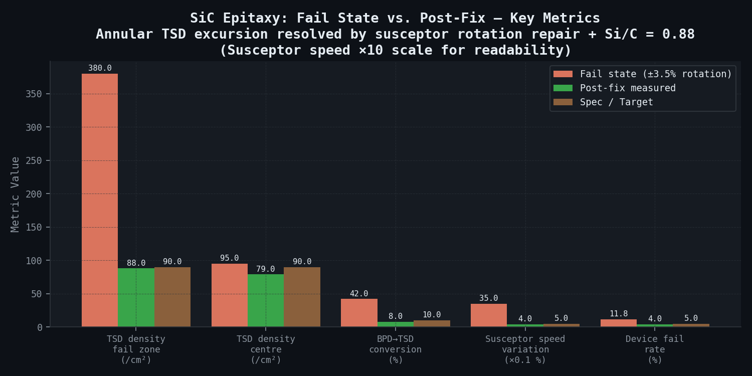
| Metric | Post-deployment (fail state) | Remediation Prediction | Post-fix Measured | Specification |
|---|---|---|---|---|
| TSD density in 15--35 mm zone | 380 cm⁻² | 85 cm⁻² | 88 cm⁻² | <90 cm⁻² |
| TSD density in centre zone | 95 cm⁻² | 82 cm⁻² | 79 cm⁻² | <90 cm⁻² |
| Si/C excursion range in fail zone | 0.80--1.18 | 0.83--0.91 (after fix) | Not directly measured | 0.85--0.95 (target) |
| BPD-to-TSD conversion rate | 42% of available BPDs | 8% (historical baseline level) | -- | <10% |
| Susceptor speed variation | +/-3.5% | +/-0.5% (after repair + PID retune) | +/-0.4% (confirmed post-repair) | <+/-0.5% |
| Device reverse recovery fail rate | 11.8% | 3.6% | 4.0% | <5% (automotive spec) |
| Fail zone annular radius | 15--35 mm from edge | Peak TSD at 22 mm | 18--28 mm (EPD measurement) | -- |
BPD-to-TSD conversion probability vs. Si/C ratio (MD/kMC simulation results):
| Si/C Ratio | BPD-to-TED Conversion (%) | BPD-to-TSD Conversion (%) | BPD Persisting (%) | Predicted TSD Density (cm⁻²) |
|---|---|---|---|---|
| 0.80 | 55% | 38% | 7% | 320 |
| 0.85 | 72% | 21% | 7% | 175 |
| 0.88 | 83% | 9% | 8% | 76 |
| 0.90 | 89% | 5% | 6% | 42 |
| 0.95 | 91% | 4% | 5% | 34 |
| 1.00 | 87% | 8% | 5% | 67 |
| 1.10 | 68% | 25% | 7% | 210 |
| 1.18 | 52% | 41% | 7% | 345 |
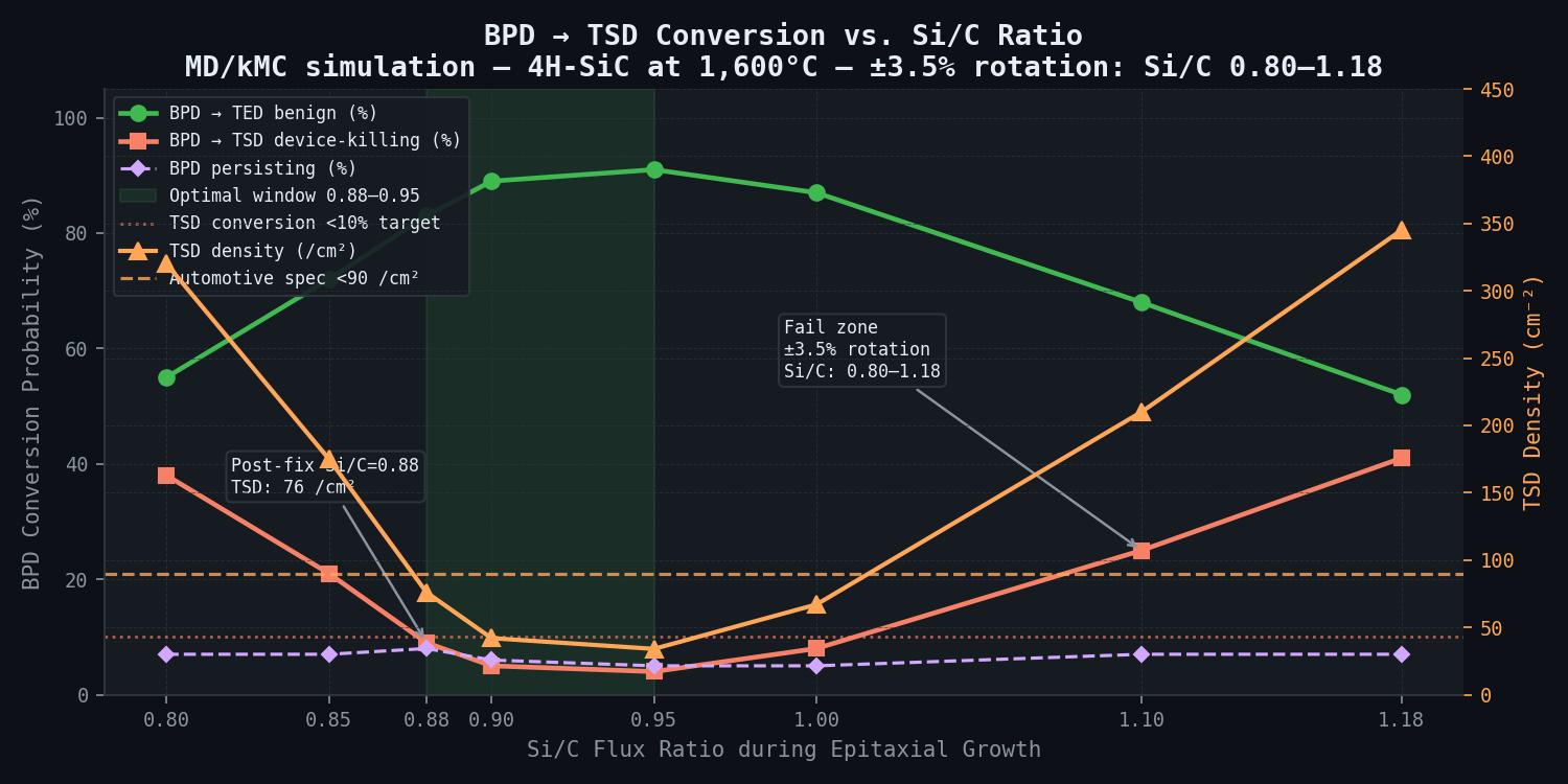
Both Si-rich (Si/C > 1.05) and C-rich (Si/C < 0.85) conditions elevate TSD conversion probability, but through different mechanisms. The optimal window (0.88--0.95) minimises TSD formation. The +/-3.5% susceptor rotation variation drives the edge-zone Si/C into both the Si-rich and C-rich regimes during speed transients, producing elevated TSD in the annular zone from both mechanisms.
Comparison Methodology
The primary validation compares higher-fidelity MD/kMC dislocation simulation and CVD reactor modelling against lower-fidelity wafer-level metrology (KOH EPD maps, profilometry, device electrical test). Published conversion fraction data provides secondary confirmation.
| Validation metric | Simulation | Measured reference | Agreement |
|---|---|---|---|
| Annular fail zone peak radius | 22 mm from edge (predicted) | 18--28 mm (KOH EPD maps) | Within +/-5 mm of peak position |
| BPD-to-TSD conversion vs. Si/C | MD/kMC curve (table above) | Published conversion fractions: within 15% | Within model uncertainty |
| CVD Si/C radial profile | Si/C range 0.80--1.18 (+/-3.5% rotation) | Epi thickness map: +/-0.8% radial variation (consistent with Si/C model) | Consistent |
| Epi thickness uniformity | 0.8% wafer variation predicted | Stylus profilometry: 0.9% +/- 0.2% | Within 0.2% absolute |
| Post-fix TSD density | 85 cm⁻² predicted | 88 cm⁻² measured (first 4-lot run after repair) | Within 3 cm⁻² (4% relative) |
| Post-fix device fail rate | 3.6% predicted | 4.0% measured (first 4-lot production run) | Within measurement uncertainty at lot sample size |
Post-fix validation covered a 4-lot production run (total 80 wafers) on the repaired susceptor with adjusted Si/C = 0.88 and tightened rotation control (+/-0.4% achieved vs. +/-0.5% specification). KOH EPD maps on 8 selected wafers (2 per lot) and device final test on all wafers confirmed TSD density and device fail rate both within specification; the spatial pattern of the annular fail zone was eliminated.
Deliverables
-
Yield signature analysis report: Spatial correlation maps (TSD density vs. device fail probability); Moran's I spatial autocorrelation analysis; hypothesis ranking scorecard with statistical significance (p-values) and confidence assignments for each hypothesis; definitive rejection of substrate-cause hypothesis with statistical support.
-
CVD reactor flux model: Si/C ratio maps at wafer surface for baseline (stable rotation) and susceptor speed variation scenarios; radial and azimuthal profiles; delivered as 2D contour maps + CSV radial profiles. Sensitivity analysis: Si/C map vs. rotation speed variation amplitude (+/-0.5%, +/-1.0%, +/-2.0%, +/-3.5%).
-
Dislocation simulation report: BPD-to-TSD conversion probability vs. Si/C ratio table and curves (MD/kMC results); TSD density vs. radius for pre- and post-fix conditions; mechanistic explanation of conversion pathway (role of partial dislocation contraction and screw character stability at high Si/C).
-
Root cause attribution document: Quantitative causal chain -- susceptor speed variation +/-3.5% to Si/C excursion 0.80--1.18 to BPD-to-TSD conversion 42% to TSD density 380 cm⁻² to device failure 11.8% -- with confidence intervals and alternative hypothesis assessment.
-
Remediation specification: Susceptor rotation control requirement (+/-0.5%), Si/C operating point (0.88 +/- 0.03), temperature uniformity requirement (+/-3 degrees C across wafer); growth rate window (7.5--8.5 um/hr); process control chart limits for TSD density monitoring by KOH EPD.
-
Post-fix validation protocol: Recommended EPD mapping frequency (1 wafer/lot during ramp, then 1 wafer/5 lots at steady state); wafer sampling positions (annular zone 15--40 mm specifically); go/no-go criteria (TSD <90 cm⁻² in annular zone, device fail rate <5%); SPC chart limits for rotation speed variance telemetry.
Timeline: 8--10 weeks from receipt of EPD maps, device fail maps, CVD reactor telemetry data (rotation speed logs for all production lots), and reactor geometry (drawing or vendor datasheet for CFD geometry construction).
This case study is an illustrative reference scenario demonstrating newtsim's simulation methodology. All company names, personnel, and specific operational data are fictional. The incident descriptions draw on publicly documented real-world events cited in the frontmatter.