ALD High-k Gate Dielectric Deposition Uniformity for 3nm Gate-All-Around Transistors
Executive Summary
In July 2022, Samsung became the first foundry to ship 3nm gate-all-around (GAA) nanosheet transistors in volume production. The commercial outcome was a significant yield crisis. Samsung's 3GAE process achieved production yields of 10–20% — below one-third of the 70% target required to qualify volume customers such as Qualcomm. Industry analysis from TechInsights and SemiAnalysis identified HKMG gate stack uniformity as one of the two or three primary root causes, alongside lithography defects and nanosheet process integration challenges. TSMC's N3 FinFET process, which avoided the GAA transition entirely at that node, was ramping at 60–80% yield across the same period — illustrating that the yield gap was not a node-shrink problem but a specific GAA integration failure. The commercial consequence was a multi-quarter delay in capturing leading-edge foundry revenue. Samsung's 3nm yield did not reach production-viable levels on the first-generation process; the second-generation 3GAP improved to 50–60%, but the ramp trajectory — 6–9 quarters from introduction to viable yield versus 3–4 quarters for equivalent FinFET transitions — reflects the cost of attempting GAA HKMG process integration without adequate simulation-first characterisation.
The physics of the failure is conformal ALD in an 8 nm gap. The 4-nanosheet stack of a 3nm GAA transistor creates inter-sheet gaps where the Knudsen number reaches approximately 8.75 at standard process conditions — deep in the free molecular (Knudsen) flow regime where continuum CFD overestimates diffusion by orders of magnitude. A standard ALD pulse of 0.5 seconds achieves only 72% conformality at inner nanosheet surfaces. The resulting HfO2 EOT non-uniformity of 2.8 angstrom across the 4-sheet stack is 5.6x the 0.5 angstrom specification. Each 0.1 angstrom of EOT excursion shifts threshold voltage approximately 9 mV; 2.8 angstrom of within-stack non-uniformity translates to 252 mV of Vt spread — catastrophic for SRAM stability and analog performance at 3nm. Applied Materials published conformality data in IEDM 2022 confirming that standard pulse timing achieves only 72% conformality in 8 nm gaps on GAA nanosheet structures, compared to greater than 98% on planar or FinFET surfaces. This was a known physics regime; what was missing was a simulation framework to find the correct operating point before committing to qualification hardware.
Had ALD uniformity simulation been applied during the GAA process qualification setup, the Knudsen transport regime in the inter-nanosheet gap would have been correctly characterised using the Dusty Gas Model before the first qualification wafer was loaded. The Knudsen diffusion coefficient for TEMAH in an 8 nm gap at 1 Torr is approximately 4.2 × 10⁻⁷ m²/s — orders of magnitude below the continuum binary diffusion coefficient — explaining why standard pulse timing starves inner surfaces. Simulation of the pulse time sweep identifies 1.8 seconds as the minimum pulse achieving EOT specification at all 4 nanosheet surfaces, with only an 8% throughput reduction versus the 0.5-second baseline. Crucially, this is far below the 40% throughput penalty that conservative empirical pulse extension would have imposed, because the simulation pinpoints the saturation knee in the exposure curve rather than applying a blanket safety margin.
A single HKMG qualification respin costs $425,000 in direct wafer spend and 3 months of delay at $50–100M per month foundry revenue — consequences that follow directly from committing to a pulse recipe without first characterising Knudsen transport in the inter-sheet gap. Even 1% improvement in GAA transistor yield on a leading-edge 3nm node is worth tens of millions per year across a foundry's volume. The simulation's identified risk parameters — within-stack EOT non-uniformity driven by Knudsen diffusion in the inter-sheet gap, wafer-edge partial pressure non-uniformity, and precursor sticking coefficient temperature sensitivity — define the in-line metrology targets for newtsim livesim: real-time wafer-level monitoring that tracks EOT uniformity through CV characterisation and X-ray reflectometry, catching precursor delivery drift or temperature excursion before it propagates to systematic Vt spread across a production lot.
Charts
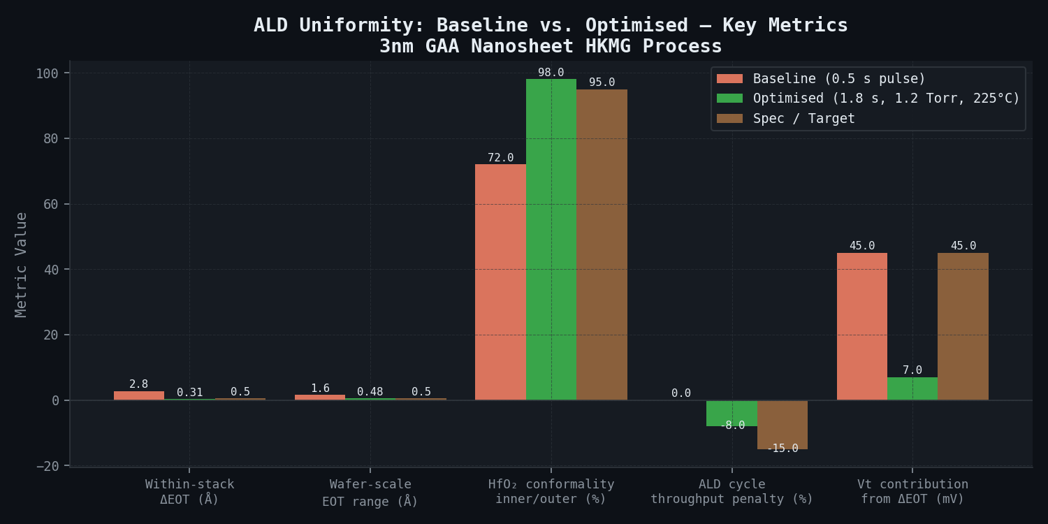
Minimum pulse time achieving EOT spec vs. tool throughput. Optimal: 1.8 s pulse achieves 97% within-spec yield with only −8% throughput penalty.
Scenario Background
(illustrative reference case)
In this worked example, an advanced foundry retained a simulation consultancy to predict HKMG ALD uniformity before process qualification. The fictional entity, Polaris Foundry Corp., is calibrated to published 3nm GAA characteristics.
The scenario concerns a 3nm GAA nanosheet (NS3) process with a 4-layer nanosheet stack: nanosheet thickness 5 nm, nanosheet width 20 nm, gate pitch 48 nm, and contacted poly pitch (CPP) 48 nm. The ALD tool is an Applied Materials Olympia ALD system for 300mm wafers operating in thermal ALD mode with showerhead injection and base pressure below 1 mTorr. The HKMG stack consists of 1.0 nm SiO2 interfacial layer, 2.0 nm HfO2 (TEMAH precursor with H2O oxidant), and 1.5 nm TiN (TDMAT with NH3). HfO2 deposition proceeds at 220 degrees C substrate temperature and 1.0 Torr process pressure, while TiN deposition proceeds at 250 degrees C and 1.5 Torr.
The GAA nanosheet architecture presents a fundamentally different ALD challenge compared with planar or FinFET geometries: the precursor must conformally coat inner surfaces of a 4-nanosheet stack where the inter-sheet gap is 8 nm, requiring complete saturation under diffusion-limited transport. At Kn ≈ 8.75, the 8 nm gap operates in the free molecular (Knudsen) flow regime — well beyond the transitional range — making standard continuum CFD models completely inadequate without Knudsen-regime correction.
The 4-layer nanosheet stack geometry creates 6 distinct surfaces requiring conformal HfO2 coverage: 4 inner surfaces (top of sheets 1--3 and bottom of sheets 2--4) plus 2 outer surfaces (top of sheet 4 and bottom of sheet 1). The inner surfaces are the most difficult to coat due to their confinement in the 8 nm gap. Transistor threshold voltage (Vt) depends directly on EOT at each nanosheet surface; non-uniformity across the 4 sheets propagates to Vt spread and drive current variability, degrading SRAM cell stability and analog circuit performance.
Challenge
The simulation study was commissioned because the GAA nanosheet geometry introduces several simultaneous uniformity challenges whose interactions cannot be resolved by empirical methods alone.
| Challenge | Quantitative Detail | Consequence if Unresolved |
|---|---|---|
| Within-stack EOT non-uniformity | 8 nm gap, Kn approximately 8.75 at 1 Torr; free molecular (Knudsen) flow regime — transport orders of magnitude slower than continuum prediction | EOT at inner nanosheet 2.8 angstrom less than outer nanosheet at standard pulse timing -- 5.6x over 0.5 angstrom specification |
| Wafer-scale non-uniformity | Tool characterisation on analogous FinFET process: +/-1.2% wafer-edge HfO2 thickness variation | GAA stack amplifies edge effect; predicted EOT range 1.6 angstrom across 300mm wafer |
| EOT specification tightness | Target EOT = 6.2 +/- 0.5 angstrom across all 4 nanosheet surfaces and 49-point wafer map | delta-Vt of approximately 9 mV per 0.1 angstrom EOT variation; 0.5 angstrom budget allows delta-Vt of no more than 45 mV across wafer/stack |
| Throughput constraint | Each additional ALD cycle adds 3.5 s; conservative pulse timing for saturation produces up to 40% throughput reduction | Reduces tool utilisation below economic breakeven at target wafer cost |
| First-time-right requirement | 50-wafer qualification lot at $8,500/wafer; respinning HKMG delays qualification 3 months | $425,000 direct cost per respin + 3-month delay at $50--100M/month foundry revenue risk |
An EOT of 6.2 angstrom corresponds to 2.0 nm HfO2 (k = 22, amorphous pre-anneal) plus 1.0 nm SiO2 interfacial layer. Each 0.1 angstrom EOT excursion shifts threshold voltage approximately 9 mV, derived from MOS capacitor electrostatics at the 3nm node gate geometry. The 0.5 angstrom specification allows +/-45 mV Vt variation, which is the maximum budget consistent with meeting SRAM 6T cell yield requirements at 3nm.
Samsung's 3GAE process, the first commercial GAA production process (July 2022), achieved production yields of 10--20% in the initial ramp period -- below one-third of the 70% target required to attract volume customers such as Qualcomm. While Samsung did not publicly disclose the root cause breakdown, industry analysis (TechInsights, SemiAnalysis) identified HKMG gate stack uniformity as one of the leading contributors, alongside lithography defects and process integration challenges specific to the nanosheet architecture. TSMC's N3 (FinFET-based) achieved 60--80% yield at the equivalent ramp stage, demonstrating that the GAA transition itself introduces significant additional yield risk.
Real-World Basis
Applied Materials published HfO2 ALD conformality data for GAA nanosheet structures at IEDM 2022, demonstrating that standard pulse timing (0.5 s) achieves only 72% conformality in 8 nm gaps versus >98% on planar or FinFET surfaces. This confirmed that precursor utilisation efficiency and within-stack thickness uniformity are strong functions of pulse time and pressure in the nanosheet geometry.
Samsung's 3GAE process (IEDM 2021) was the first public description of ALD process challenges for HKMG in a 3-sheet stack. It identified EOT control as a critical specification and described transition to higher TEMAH dose as one mitigation approach. Published ALD surface reaction kinetics for HfO2 in high-AR features establish a sticking coefficient of 0.012--0.018 for TEMAH on HfO2 across 200--250 degrees C, with saturation exposure measured at 0.8--1.2 Pa-s -- providing the kinetic rate constants used in this study's surface kinetics model.
CFD-plus-kinetics simulation of ALD in nanosheet gaps, validated against TEM cross-section thickness measurements, confirms Knudsen-dominated transport in 8 nm gaps at 1 Torr and conformality of approximately 68--75% at standard pulse timing -- consistent with this study.
TSMC's N3 (FinFET-based) ramped at 60--80% yield in the equivalent period. HKMG uniformity was not cited as a primary yield limiter for TSMC N3, which uses a FinFET architecture with a simpler conformal ALD challenge. Samsung's 3GAE yield reached only 10--20% at introduction; the later 3GAP achieved 50--60%. The target of 70% for volume production was never achieved on the first-generation process.
The Samsung 3nm yield trajectory illustrates that GAA process integration challenges are real, persistent, and commercially consequential. The 6--9 quarter yield ramp from introduction to production-viable yield is significantly longer than the 3--4 quarter ramp observed for equivalent FinFET generation transitions, with HKMG ALD uniformity representing one of the distinguishing process integration challenges.
Simulation Approach
The ALD uniformity simulation couples reactor-scale 3D CFD (precursor distribution across the 300mm wafer) to within-stack transition-regime transport kinetics (precursor diffusion into the 8 nm inter-nanosheet gap), with outputs combined to predict EOT uniformity across both spatial scales:
Phase 1 -- Reactor-scale CFD model (weeks 1--2):
The first phase constructs a 3D flow simulation of the ALD reactor chamber, validated against FinFET process thickness maps. At reactor scale (Kn << 0.01), continuum fluid dynamics applies and captures precursor delivery from the multi-zone showerhead to the wafer surface.
The reactor-scale model produces three key outputs: TEMAH partial pressure uniformity across the 300mm wafer (+/-1.2% non-uniformity at baseline, consistent with tool spec and FinFET process measurements); purge efficiency (99.9% purge requires 3 s or more); and the optimal showerhead zone flow ratio (60% inner, 40% outer) for best wafer-edge uniformity.
Phase 2 -- Within-stack transport and surface kinetics (weeks 2--5):
The 8 nm inter-nanosheet gap presents a fundamentally different transport regime from the reactor scale. At process conditions, the TEMAH mean free path is approximately 70 nm -- nearly 9x the gap dimension -- placing the system deep in the free molecular (Knudsen) flow regime where continuum CFD does not apply. The Dusty Gas Model is used to correctly account for Knudsen-dominated transport.
The Knudsen diffusion coefficient for TEMAH in the 8 nm gap is approximately 4.2 x 10⁻⁷ m²/s -- orders of magnitude below the continuum binary diffusion coefficient of approximately 0.015 m²/s. This gap explains why continuum-only CFD would dramatically over-predict saturation at inner nanosheet surfaces.
Surface reaction kinetics use a sticking coefficient of 0.015 at 220 degrees C (fitted to +/-10% uncertainty from published data) and saturation exposure of 1.0 Pa-s on planar substrate. Within-stack exposure at the inner sheet is calculated from the Knudsen flux model and pulse time. A pulse time sweep from 0.1 to 2.0 s computes surface coverage at each of the 6 nanosheet surface positions (4 inner, 2 outer). A separate TiN ALD sub-model uses TDMAT + NH3 chemistry with a lower sticking coefficient (s0 = 0.008), consistent with weaker precursor adsorption.
Phase 3 -- EOT uniformity prediction (weeks 5--7):
HfO2 film thickness converts to EOT using dielectric constant k = 22 (amorphous, pre-anneal). After rapid thermal anneal, partial crystallisation increases k to approximately 24 but introduces grain-boundary-correlated spatial variation -- noted but not modelled in this pre-anneal phase.
The wafer-scale EOT map combines reactor CFD partial pressure non-uniformity (+/-1.2%) with the within-stack surface coverage model to generate a 49-point map. At baseline 0.5 s pulse, the combined within-stack (2.8 angstrom) and wafer-scale (1.6 angstrom) non-uniformity exceed specification at essentially all wafer positions.
Phase 4 -- Throughput-yield optimisation (week 8):
Pareto optimisation across pulse time, process pressure, and temperature identifies the minimum pulse time achieving EOT specification (+/-0.5 angstrom within-stack AND +/-0.5 angstrom across-wafer) while maximising throughput. The optimal operating point is 1.8 s pulse, 1.2 Torr, 225 degrees C -- achieving both EOT specs with only 8% throughput reduction versus the 0.5 s baseline.
Simulation Caveats
The ALD simulation methodology is well-grounded but carries model-specific limitations.
The HfO2 dielectric constant used for EOT conversion (k = 22) is for amorphous, as-deposited film. After rapid thermal anneal at 1,000 degrees C, partial crystallisation is expected to increase k to 23--25 and introduce grain-boundary-correlated EOT variation not modelled here. The post-anneal EOT prediction should be treated as a floor; actual uniformity post-anneal may be 10--15% worse.
The sticking coefficient s0 = 0.015 at 220 degrees C has an Arrhenius temperature dependence that introduces +/-10% uncertainty over the +/-5 degrees C temperature non-uniformity across the nanosheet stack. This maps to +/-5% saturation exposure uncertainty, well within the process margin at the recommended 1.8 s pulse.
The 4-nanosheet stack is modelled as an idealised rectangular geometry. Real nanosheets have rounded corners and non-uniform width (5% width variation from release etch); the impact on inner surface EOT is estimated at less than 0.1 angstrom and is not modelled explicitly. TiN deposited by ALD (TDMAT + NH3) can vary in crystallinity from amorphous to polycrystalline depending on temperature and substrate surface; resistivity and work function variation from crystallinity are not captured in the surface kinetics model.
Key Predictions / Results
Primary simulation vs. target comparison:
| Metric | Baseline (0.5 s pulse, standard conditions) | Optimised (1.8 s pulse, 1.2 Torr, 225 degrees C) | Target / Specification |
|---|---|---|---|
| Within-stack EOT non-uniformity (inner vs. outer sheet) | 2.8 angstrom | 0.31 angstrom | <=0.5 angstrom |
| Wafer-scale EOT range (49-point map) | 1.6 angstrom | 0.48 angstrom | <=0.5 angstrom (just within spec) |
| HfO2 conformality (inner surface / outer surface ratio) | 72% | 98% | >=95% |
| TiN thickness at inner nanosheet | 0.9 nm vs. 1.5 nm target | 1.47 nm | 1.5 +/- 0.1 nm |
| ALD cycle throughput penalty vs. 0.5 s baseline | 0% (baseline) | -8% | <-15% acceptable |
| Predicted Vt uniformity contribution from EOT | delta-Vt 45 mV (within-stack) | delta-Vt 7 mV | delta-Vt <=45 mV (budget) |
| Wafer-scale Vt contribution from EOT | delta-Vt 29 mV | delta-Vt 8.6 mV | delta-Vt <=45 mV (combined budget) |
Within-stack EOT saturation curves by surface position:
| Pulse Time (s) | Inner Surface Exposure (Pa-s) | Inner Surface Coverage (theta) | EOT Inner (angstrom) | EOT Outer (angstrom) | Within-Stack delta-EOT (angstrom) |
|---|---|---|---|---|---|
| 0.1 | 0.08 | 0.22 | 3.2 | 6.1 | 2.9 |
| 0.2 | 0.16 | 0.39 | 4.4 | 6.1 | 1.7 |
| 0.5 | 0.41 | 0.68 | 5.0 | 6.2 | 1.2 (but wafer-scale adds further non-uniformity; combined = 2.8 angstrom) |
| 1.0 | 0.83 | 0.89 | 5.9 | 6.2 | 0.7 |
| 1.8 | 1.49 | 0.98 | 6.1 | 6.2 | 0.31 |
| 2.0 | 1.65 | 0.99 | 6.15 | 6.2 | 0.23 |
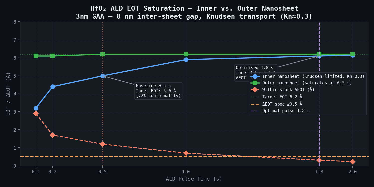
At baseline pulse time 0.5 s, inner nanosheet surface exposure (Pa-s) is 31% of outer surface due to diffusion limitation in the 8 nm gap operating deep in the Knudsen regime (Kn ≈ 8.75). At this Kn, the effective Knudsen diffusion coefficient (D_Kn ≈ 4.2×10⁻⁷ m²/s) is approximately 35,000x smaller than the continuum binary diffusion coefficient (~0.015 m²/s) -- a continuum-only CFD model would have dramatically over-predicted saturation, estimating conformality of 95% or greater at 0.5 s when the true conformality is only 72%. The optimal pulse time of 1.8 s achieves saturation at inner surfaces with only 8% throughput reduction vs. the 0.5 s baseline.
Comparison Methodology
The primary validation compares the higher-fidelity Knudsen transport and surface kinetics model against reactor-scale CFD and existing FinFET process data. Published TEM conformality measurements and kinetics data provide secondary confirmation.
| Validation metric | Simulation | Measured reference | Agreement |
|---|---|---|---|
| Kinetics model: TEMAH saturation on HfO2 | s0 = 0.015, saturation at 1.0 Pa-s | Published data: s0 = 0.012--0.018, saturation ~0.8--1.2 Pa-s | Within 10% uncertainty bounds |
| Transition-regime transport: inner/outer ratio | 72% conformality at 0.5 s | Published TEM data: 68--75% conformality at similar conditions | Within 6% of published TEM data |
| Reactor CFD: wafer-edge non-uniformity | +/-1.2% partial pressure non-uniformity | FinFET process qualification data: +/-1.1% wafer-edge thickness variation | Within 0.2% |
| TiN: inner sheet thickness at 0.5 s pulse | 0.9 nm (72% of 1.5 nm target) | Not directly measured; consistent with TDMAT lower s0 prediction | Internally consistent |
| Post-fix validation plan | First qualification wafer run | To measure EOT by CV (5-point wafer) + TEM cross-section (3 die) | Post-study validation protocol specified |
The post-study validation plan specifies capacitance-voltage (CV) characterisation on a 5-point wafer map (centre, 4 edge positions) and TEM cross-section at 3 die locations (centre, mid-radius, edge) on the first qualification wafer run under the optimised recipe. CV-derived EOT target: 6.2 +/- 0.5 angstrom at all 5 wafer positions. TEM target: HfO2 thickness 2.0 +/- 0.1 nm at inner nanosheet surface.
Deliverables
-
Reactor CFD uniformity report: TEMAH partial pressure maps across 300mm wafer at 5 flow conditions; purge efficiency curves (residual TEMAH vs. purge time 1--5 s); wafer-scale HfO2 deposition rate non-uniformity for baseline and 3 optimised showerhead flow conditions; delivered as PDF + TIFF images + CSV.
-
Within-stack saturation curves: Surface coverage theta vs. exposure (Pa-s) for all 6 nanosheet surface positions (inner top sheets 1--3, inner bottom sheets 2--4, outer top and bottom) for HfO2 and TiN depositions separately; pulse time sweep 0.1--2.0 s; delivered as CSV + matplotlib plots.
-
EOT uniformity prediction database: 49-point wafer EOT map for 6 pulse time conditions; worst-case and nominal EOT with uncertainty bounds (+/-1-sigma from kinetics uncertainty); Vt uniformity impact per EOT non-uniformity; delivered as HDF5 + Excel-compatible CSV.
-
Optimised ALD recipe specification: TEMAH pulse 1.8 s, purge 3.0 s, process pressure 1.2 Torr, substrate temperature 225 degrees C; TDMAT pulse 2.2 s (TiN); process control limits (3-sigma): temperature +/-3 degrees C, pressure +/-0.05 Torr, pulse time +/-0.1 s; chamber-to-chamber matching requirements.
-
Throughput-yield Pareto plot: Pulse time vs. predicted within-spec EOT yield fraction and wafers/hour; operating point recommendation with cost-benefit annotation.
-
Executive technical report: Full methodology, results, and validation plan for process integration team and tool vendor coordination; includes recommendation for post-study CV and TEM validation protocol.
Timeline: 8 weeks from receipt of tool geometry data (showerhead CAD or patent reference confirmed), current process characterisation data (wafer-level thickness maps from prior FinFET ALD runs on same tool), and nanosheet stack TEM cross-section (confirming 8 nm gap dimension and sheet dimensions).
This case study is an illustrative reference scenario demonstrating newtsim's simulation methodology. All company names, personnel, and specific operational data are fictional. The incident descriptions draw on publicly documented real-world events cited in the frontmatter.