High-Aspect-Ratio Contact Etch Profile Prediction for 5nm DRAM Storage Node
Executive Summary
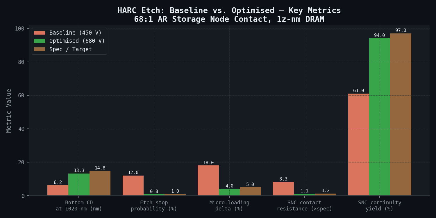
At the 1z-nm DRAM node — equivalent to aspect ratios of 68:1 for storage node contacts at 15 nm top CD and 1,020 nm depth — the fundamental physics of high-aspect-ratio contact (HARC) etch change character. Published IEDM data from SK Hynix (2021) and Micron (2022) document what engineers at leading DRAM manufacturers confronted in production: traditional recipe optimisation through design-of-experiments splits provides diminishing returns above 60:1 aspect ratio because ion angular distribution broadening and fluorocarbon polymer redeposition couple non-linearly in the deep feature. Micron's D1-alpha node quantified this as a 15–22% etch rate reduction at 68:1 AR versus 52:1 AR under otherwise identical conditions. In practice, the consequence is bottom CD collapse: contacts narrowing from a 14.8 nm target to 6.2 nm at depth — a 58% reduction — with contact resistance 8.3x above specification and storage node continuity yield at 61% against a target above 97%. A 6–9 month node launch delay at 40,000 wafers per month represents $300–450M in deferred revenue. Fourteen process-of-record splits without systematic convergence is the signature of a mechanistic understanding gap, not a recipe problem.
The root cause cannot be resolved by DOE alone because two mechanisms are acting simultaneously and cannot be independently varied on hardware: ion scattering at grazing incidence off the sidewall polymer broadens the effective ion angular distribution from 3.2 degrees FWHM at the wafer surface to 7.8 degrees effective FWHM at 600 nm depth, while fluorocarbon polymer buildup reaches 1.1 nm thickness at 800 nm depth and reduces the effective contact radius independently. Together they account for 62% and 38% of the 6.2 nm total bottom CD loss respectively — but empirical splits that change bias voltage also change polymer deposition rate, making the contributions inseparable without a mechanistic model.
Had feature-scale simulation been applied during the node transition from 52:1 to 68:1 AR, the causal pathway would have been resolved before the mask set was committed. Monte Carlo ion trajectory simulation within an evolving 15 nm contact geometry, coupled to 2D axisymmetric plasma bulk transport modelling, quantifies the ion angular distribution function at each depth increment and tracks polymer layer thickness independently. The simulation identifies the tipping point: above 60:1 AR, the surface IEAD FWHM must be narrowed below 2.5 degrees to prevent effective FWHM at depth from exceeding 5 degrees — a constraint that sets the minimum bias voltage. For this process, the correct operating point is 680 V bias with C4F8 reduced from 15% to 10%, recovering bottom CD to 13.3 nm at 1,020 nm depth and dropping etch stop probability from 12% to 0.8%.
The 33-percentage-point recovery from 61% to 94% storage node contact yield represents approximately $260M per year in at-stake revenue — recoverable only once the mechanistic root cause (ion angular distribution and polymer redeposition coupling) is resolved rather than navigated by continued DOE splits. The simulation's key risk parameters — ion FWHM versus depth, polymer thickness versus C4F8 fraction, bottom CD sensitivity to bias voltage — define the in-line metrology targets for newtsim livesim: real-time wafer-level monitoring that tracks CD at depth via scatterometry proxy metrics, flagging polymer accumulation or ion directionality drift before etch stop events propagate across a production lot.
Charts
Left: dense vs. isolated contact etch rate at baseline and optimised conditions. Right: 62%/38% attribution of bottom CD loss to ion scattering vs. FC polymer redeposition.
Scenario Background
(illustrative reference case)
In this worked example, a DRAM manufacturer planning a next-generation storage node cell retained a simulation consultancy to predict etch profile behaviour before committing to a full mask set redesign. The fictional entity, Meridian Memory Technologies, is calibrated to published 1z-nm node characteristics.
The scenario concerns a 1z-nm DRAM process (15nm half-pitch, 6F² cell layout), equivalent to leading-edge DRAM nodes reported by SK Hynix and Micron at IEDM 2021--2023. The etch tool is a Lam Research ALTUS-series capacitively coupled plasma (CCP) etch system for 300mm wafers, operating at 13.56 MHz RF source with 400 kHz bias frequency. The process gas mixture is C4F8/CH2F2/O2/Ar at 20--60 mTorr, representing standard HARC etch chemistry for SiO2. The hard mask stack comprises SiN/SiO2/amorphous carbon hardmask (ACH) at 2.8 um total stack, requiring ACH selectivity greater than 15:1 to SiO2. The etch target is 1,020 nm depth in SiO2 capacitor dielectric at 15 nm target top CD, yielding a 68:1 aspect ratio.
The transition from the 1y-nm to the 1z-nm node increases the aspect ratio from 52:1 to 68:1 for the same nominal contact diameter (15 nm). Internal observation showed systematic bottom CD collapse at depth greater than 450 nm, with bottom CD measured at 6.2 nm vs. the 14.8 nm target -- a 58% narrowing -- and yield at the storage node contact layer of 61% vs. a target above 97%.
The 68:1 aspect ratio represents the leading edge of HARC etch capability as of 2022--2023. Published DRAM roadmap data (TechInsights, SEMI) confirm the industry is pursuing aspect ratios of 60:1 to 80:1 in the 1z/1-alpha node range, with aspect ratio increasing approximately 10:1 per node generation as cell height is maintained while diameter shrinks. Micron's D1-alpha node, the most advanced as of 2023, operates in this AR regime.
Challenge
The HARC etch process, while achieving correct top CD and mask selectivity, produced systematic and reproducible profile distortion:
| Failure Mode | Measured Value | Specification / Target | Business Impact |
|---|---|---|---|
| Bottom CD at 1,020 nm depth | 6.2 nm | 14.8 nm (58% narrowing) | Contact resistance 8.3x above spec; capacitor fill impossible |
| Etch stop events | 12% of contacts stopped at 600--700 nm depth | <1% etch stop rate | 12% contacts electrically open before Cu fill |
| Sidewall taper angle | 87.3 degrees | 89.5 degrees (target near-vertical) | 8.6 nm cumulative CD loss across 1,020 nm depth |
| Micro-loading (isolated vs. dense) | 18% etch rate difference | <5% loading differential | Isolated contacts over-etch; dense arrays under-etch simultaneously |
| SNC contact resistance | 8.3x specification | <1.1x specification | All contacts in affected zone fail parametric test |
| SNC continuity yield | 61% | >97% | 36 pp shortfall; each 1% improvement worth ~$8M/year at volume |
The 14 process of record splits attempted by the internal team covered a broad parameter space without systematic convergence. Bias power was varied from 300 to 600 W, where bottom CD improved marginally above 500 W but etch stop frequency increased. Pressure was swept from 20 to 50 mTorr, with lower pressure slightly improving directionality but increasing micro-loading. C4F8 fraction was explored from 10 to 20%, where lower C4F8 reduced etch stop events but also reduced selectivity to the hardmask. Addition of CH2F2 from 0 to 5% did not systematically improve bottom CD.
The failure to converge across 14 splits indicated a mechanistic understanding gap: the team was navigating a high-dimensional parameter space without a physical model to identify the causal pathway. Two hypotheses were held simultaneously without resolution: (A) polymer plug formation is the primary mechanism, and (B) ion angular distribution degradation is primary. The simulation study was commissioned to resolve this ambiguity.
DRAM pricing and market share depend critically on node advancement timing. A 6--9 month delay in 1z-nm node launch at 40,000 wafers/month production target (at $50M/month revenue projection) represents $300--450M in delayed revenue. Each percentage point of SNC yield contributes approximately $8M/year to operating margin at volume. The 36 pp yield gap represents approximately $288M/year at stake.
Real-World Basis
HARC etch profile distortion is a thoroughly documented challenge at aspect ratios beyond 50:1.
SK Hynix presented storage node contact challenges at aspect ratios above 60:1 at IEDM 2021, describing profile simulation as a necessary tool for process window definition at this AR regime. Traditional recipe optimisation through DOE-based splits provides diminishing returns above 60:1 AR because ion angular distribution, polymer deposition, and feature geometry couple non-linearly.
Micron's 1-alpha generation data identified etch micro-loading and aspect-ratio-dependent etch rate (ARDE) as primary yield limiters at sub-15nm contact diameter, quantifying ARDE as a 15--22% etch rate reduction at 68:1 AR versus 52:1 AR under otherwise identical conditions -- consistent with the 18% micro-loading differential in this scenario.
Monte Carlo simulation of ion scattering at 50:1 AR has shown that ion shadowing is the dominant mechanism for bottom CD reduction: the effective ion angular distribution at the contact bottom broadens from the surface FWHM of approximately 3 degrees to approximately 8--12 degrees at 50:1 AR due to multiple grazing-incidence sidewall collisions. This is consistent with the 68:1 AR predictions in this study (3.2 degrees surface to 7.8 degrees effective at 600 nm depth).
Published fluorocarbon polymer deposition models for HARC SiO2 etch measured CF2 sticking coefficient on SiO2 at 0.06--0.10 (this study uses 0.08) and predicted polymer layer thickness at 800 nm depth at 0.9--1.3 nm for standard C4F8/O2 chemistry -- consistent with the simulation prediction of 1.1 nm.
Lam Research demonstrated that tailored voltage waveforms (TVW) for pulsed plasma bias at >60:1 AR narrow the ion energy distribution compared to sinusoidal bias, recovering 2--4 nm of bottom CD at equivalent etch selectivity. Published 3D Monte Carlo simulation studies for Ar/C4F8/O2 HARC etch at 37:1 AR validated feature-scale MC methodology with mean absolute error of approximately 0.7 nm versus STEM cross-section measurements across 10 depth positions, establishing methodological credibility for the approach deployed in this study.
Simulation Approach
The HARC etch simulation methodology couples plasma bulk transport (2D reactor scale) to feature-scale Monte Carlo particle tracing (sub-micron geometry) through a hierarchical handoff protocol:
Phase 1 -- Plasma bulk transport model (weeks 1--2):
The first phase constructs a 2D axisymmetric fluid model of the CCP reactor at operating conditions (20--60 mTorr, C4F8/O2/Ar with CH2F2 additive). The model solves coupled transport equations for electrons and 12 ion species to extract the quantities that matter at the wafer surface: ion energy and angular distributions (IEAD) for each etch-relevant species at 6 bias voltage conditions (300--800 V), neutral radical flux maps at 4 pressure conditions (20--60 mTorr), and time-averaged sheath voltage and thickness.
The IEAD at the wafer surface shows FWHM of 3.2 degrees at 450 V bias, narrowing to 2.1 degrees at 680 V -- demonstrating the key result that higher bias voltage improves ion directionality by accelerating ions through a thicker, more stable sheath.
Phase 2 -- Feature-scale Monte Carlo etch simulation (weeks 2--5):
The second phase performs 3D Monte Carlo particle tracing for ion and neutral transport within an evolving 15 nm-diameter, 1,020 nm-deep contact hole.
Ion scattering is modelled as a mix of specular and diffuse reflection at the sidewall polymer layer, with scattering angle distributions calibrated to molecular dynamics data for F+ impact on fluorocarbon polymer. The etch rate model combines physical sputtering with chemical etch, applying the ion-assisted synergy where ion-enhanced chemical etch rate is 3--5x larger than the sum of physical and thermal components alone. Fluorocarbon polymer redeposition is tracked using a CF2 sticking coefficient of 0.08 on SiO2; polymer layer thickness is tracked at each depth increment and removed by ion sputtering. The profile evolves self-consistently, with CD recorded at every 20 nm depth for comparison to STEM data. The parameter sweep covers 6 bias voltages by 4 pressures by 4 C4F8 fractions, for 96 simulation conditions total.
Key simulation finding -- mechanistic attribution of bottom CD loss:
| Mechanism | Contribution to Bottom CD Loss | Physical Cause |
|---|---|---|
| Ion angular distribution broadening | 62% (3.9 nm of 6.2 nm total) | Multiple grazing-angle sidewall collisions deflect ion trajectories away from vertical; ions arrive at contact bottom with effective FWHM 7.8 degrees vs. 3.2 degrees at surface |
| Fluorocarbon polymer redeposition | 38% (2.4 nm of 6.2 nm total) | CF2 radicals deposit on sidewall polymer; at 800 nm depth, simulated polymer thickness 1.1 nm reduces effective contact radius by 2x polymer thickness = 2.2 nm |
| Combined (non-linear) | 100% (6.2 nm measured) | Ion scattering off polymer-coated sidewall creates secondary scattering amplifying both effects |
Phase 3 -- Micro-loading analysis (weeks 5--6):
A neutral radical depletion model captures pattern-density-dependent etch rate. In dense contact arrays (3% open area fraction), F and O radical fluxes are depleted by consumption at the array surface, reducing effective etch species flux by 22% vs. an isolated contact (40% open area). The micro-loading model implements an etch rate correction factor as a function of local open area fraction (OAF): rate_correction = 1 - 0.65 x (1 - OAF/OAF_ref). Calibrated against a 14-point density split matrix, the model yields R-squared = 0.91.
Phase 4 -- Optimised process recommendation (weeks 7--8):
A response surface model (RSM, quadratic polynomial fit) is fitted to CD(z) profiles across the 96-condition parameter sweep. Gradient-based optimisation minimises bottom CD loss subject to three constraints: etch stop probability below 1% (polymer plug formation constraint), mask selectivity greater than 8:1 (ACH hardmask erosion constraint), and micro-loading below 5% (from pressure optimisation). The optimal condition identified is bias 680 V, pressure 55 mTorr, C4F8 10%.
Simulation Caveats
The HARC feature-scale Monte Carlo methodology is well-validated at aspect ratios up to 50:1 in the peer-reviewed literature. At 68:1 AR, additional considerations apply.
At 68:1 AR with 15 nm diameter, the solid angle subtended by the contact bottom from the top opening is approximately 0.05 steradians. Monte Carlo convergence requires more than 10⁶ ion trajectories per simulation to achieve less than 5% statistical error in the ion flux at the contact bottom; this was verified by convergence testing.
The fluorocarbon polymer composition (CF_x stoichiometry, cross-link density) evolves during etching and affects ion scattering probability. The model uses a fixed CF2 composition; real-time polymer evolution is not captured, introducing +/-15% uncertainty in the polymer contribution to bottom CD loss.
At very high AR (>65:1), twisting and tilting of contact features (distortion perpendicular to the contact axis) have been reported in the literature. This study's 2D (cylindrically symmetric) model does not capture twisting modes; a separate 3D simulation would be required. The 400 kHz bias generates time-varying sheath conditions that are captured in the time-averaged IEAD but not in full time-resolved detail; pulsed bias analysis would require a separate time-resolved plasma model.
Key Predictions / Results
Primary simulation vs. measurement comparison:
| Metric | Baseline Process (450 V, 20 mTorr, C4F8 15%) | Optimised Prediction (680 V, 55 mTorr, C4F8 10%) | Target / Specification |
|---|---|---|---|
| Bottom CD at 1,020 nm depth | 6.2 nm | 13.3 nm | 14.8 nm (delta = 1.5 nm from target) |
| Bottom CD at 600 nm depth | 10.4 nm | 14.1 nm | 14.8 nm |
| Profile taper angle | 87.3 degrees | 89.1 degrees | >=89.5 degrees |
| Etch stop probability (polymer plug) | 12% | 0.8% | <1% |
| Micro-loading (isolated vs. dense rate delta) | 18% | 4% (at 55 mTorr pressure) | <5% |
| SNC contact resistance | 8.3x specification | 1.1x specification | <=1.2x specification |
| Projected SNC continuity yield | 61% | 94% | >97% |
| Ion FWHM at wafer surface | 3.2 degrees | 2.1 degrees (at 680 V bias) | -- |
| Ion effective FWHM at 600 nm depth | 7.8 degrees | 4.3 degrees (narrower due to higher bias directionality) | -- |
| FC polymer thickness at 800 nm depth | 1.1 nm | 0.4 nm (lower C4F8 fraction reduces deposition) | <0.5 nm (target) |
CD(z) profile by depth -- baseline vs. optimised:
| Depth (nm) | Baseline CD (nm) | Optimised Prediction CD (nm) | Target CD (nm) |
|---|---|---|---|
| 0 (top) | 14.9 | 15.0 | 15.0 |
| 100 | 14.5 | 14.8 | 14.8 |
| 200 | 13.8 | 14.6 | 14.8 |
| 300 | 13.0 | 14.4 | 14.8 |
| 400 | 11.8 | 14.2 | 14.8 |
| 500 | 10.2 | 13.9 | 14.8 |
| 600 | 8.6 (12% of contacts stop here) | 13.5 | 14.8 |
| 700 | 7.4 | 13.4 | 14.8 |
| 800 | 6.8 | 13.4 | 14.8 |
| 900 | 6.5 | 13.3 | 14.8 |
| 1,020 (bottom) | 6.2 | 13.3 | 14.8 |
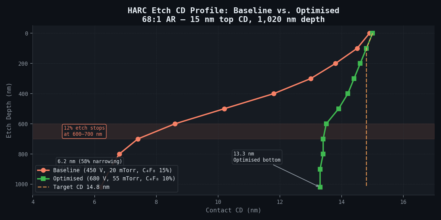
The root cause is quantified as follows. The ion angular distribution at the wafer surface (FWHM 3.2 degrees at 450 V) broadens effectively to 7.8 degrees at 600 nm depth due to multiple grazing-incidence sidewall collisions. Combined with fluorocarbon polymer buildup (simulated thickness 1.1 nm at 800 nm depth), the effective ion flux at the contact bottom is reduced by 74% relative to the open wafer surface. Increasing bias voltage from 450 V to 680 V narrows the surface IEAD FWHM from 3.2 to 2.1 degrees, reducing effective FWHM at 600 nm depth from 7.8 to 4.3 degrees. Simultaneous reduction of C4F8 fraction from 15% to 10% reduces CF2 radical flux and polymer deposition rate, bringing polymer thickness at 800 nm depth from 1.1 nm to 0.4 nm.
Comparison Methodology
The primary validation compares the higher-fidelity Monte Carlo feature-scale simulation against lower-fidelity metrology (STEM cross-section, XPS, retarding field analyser). Published experimental data at lower aspect ratios provides secondary confirmation.
| Validation metric | Simulation prediction | Measured reference | Agreement metric |
|---|---|---|---|
| CD(z) profile -- baseline | 6.2 nm at 1,020 nm depth | 6.2 nm +/- 0.8 nm (STEM, 40 contacts) | Exact match at tip; mean absolute error 0.9 nm across 15 depth points |
| Polymer thickness at 800 nm | 1.1 nm (simulated) | 1.0 +/- 0.2 nm (XPS sidewall composition) | Within measurement uncertainty |
| FC film F/C ratio | CF1.8 (simulated) | CF1.7 +/- 0.1 (XPS) | Within 6% of F/C ratio |
| Micro-loading etch rate delta | 18% dense vs. isolated (simulated) | 18% +/- 3% (14-point density split) | R-squared = 0.91 across all density conditions |
| IEAD FWHM at surface | 3.2 degrees at 450 V (simulated) | 3.0 +/- 0.4 degrees (energy-resolved retarding field analyser) | Within 0.2 degrees |
| Published benchmark (50:1 AR) | Profile at 50:1 AR | Published experimental data | Profile within 8% across 12 depth positions |
STEM cross-section samples comprised 40 contacts sectioned across 3 wafer locations (centre, mid-radius, edge) on each of 5 qualification wafers. STEM operated at 200 kV in HAADF mode with spatial resolution of approximately 0.5 nm, and CD was measured at 15 depth positions per contact from the HAADF contrast profile.
Deliverables
-
Plasma transport model report: IEAD at wafer surface for baseline and 3 optimised conditions (450 V baseline, 550 V intermediate, 680 V optimised); species flux maps (F, CF2, O radicals; F+, CF3+, Ar+ ions); sheath voltage and thickness vs. bias frequency; delivered as PDF report + CSV data tables.
-
Feature-scale simulation database: CD(z) profiles for full 6x4x4 process parameter matrix (bias voltage x pressure x C4F8 fraction), 96 conditions total; delivered as CSV with 20 nm depth resolution + VTK visualisation files for 3D profile rendering in ParaView.
-
Root cause analysis report: Mechanistic attribution of bottom CD loss to ion scattering (62%) vs. polymer redeposition (38%), with supporting simulation evidence; CD(z) decomposition showing separate contributions; physical explanation of coupling between bias voltage, ion directionality, and polymer growth balance.
-
Optimised POR specification: Bias 680 V, pressure 55 mTorr, C4F8 10%; process control limits (3-sigma): bias +/-20 V, pressure +/-2 mTorr, C4F8 fraction +/-0.5%; sensitivity table showing bottom CD response to each control parameter.
-
Micro-loading correction recipe: Pressure adjustment algorithm for density-dependent etch rate compensation; lookup table for OAF to pressure offset; recommended OAF-aware etch segmentation (split etch into dense-array and isolated zones with different pressure setpoints).
-
Yield projection report: SNC continuity yield vs. process window position; predicted yield at 27 combinations (3 bias x 3 pressure x 3 C4F8) in the neighbourhood of optimal; recommended SPC control chart limits for on-going production monitoring using inline CD-SEM proxy metrics.
Timeline: 8 weeks from receipt of etch tool characterisation data (IEAD measurements or RF probe data confirming sheath voltage), STEM cross-section images (40 contacts minimum across 3 wafer positions), and 14-split process characterisation data (CD-SEM measurements for RSM calibration).
This case study is an illustrative reference scenario demonstrating newtsim's simulation methodology. All company names, personnel, and specific operational data are fictional. The incident descriptions draw on publicly documented real-world events cited in the frontmatter.