EUV Lithography Stochastic Defect Reduction at 10nm Logic Node
Executive Summary
Between 2016 and 2019, Intel's 10nm logic node became one of the most costly yield failures in modern semiconductor history. The company publicly acknowledged multi-year yield difficulties across Q3 and Q4 2018 earnings calls, attributing losses to defect density without disclosing root cause. Industry analysis subsequently identified the primary mechanism: aggressive self-aligned quad-patterning (SAQP) accumulated overlay error of approximately 3.5 nm 3-sigma across four DUV exposures — an edge placement error budget incompatible with 10nm minimum spacing rules. Production volume was delayed by approximately 2.5 years. At 40,000 wafers per month with wafer costs in the range of $150,000 fully allocated and a 55-percentage-point yield gap, the revenue impact exceeded $385M per year. The root cause was not random — it was a systematic process window failure that deterministic optical proximity correction models, without stochastic extension, could not predict. Every additional EUV or multipatterning layer committed to an under-characterised process window carried the same catastrophic risk.
The mechanism is photon shot noise. At 30 mJ/cm² on a 32 nm pitch metal-2 layer, absorbed EUV photon flux reaches only approximately 7 photons/nm² in a chemically amplified resist at 35% absorption. Poisson statistics impose a 1-sigma fluctuation of approximately 38% per resolution element — a fundamental noise floor that drives stochastic line-edge roughness and isolated contact bridging independently of optical aberration correction. Resist acid diffusion (4 nm blur length) and mask 3D phase asymmetry compound the effect. These mechanisms are invisible to scalar Hopkins OPC models. The consequence was 4.2 bridge defects/cm² and 1.8 line-break defects/cm² at nominal conditions — 8x and 9x above the yield-model breakeven threshold respectively — and a functional die yield of 23% against a 78% production target.
Had process simulation been applied during EUV process development at this node, the stochastic regime would have been characterised before committing to a process of record. Monte Carlo photon absorption simulation, coupled with stochastic acid-diffusion resist modelling and source-mask optimisation, identifies the dose threshold at which absorbed photon count per resolution element is sufficient to suppress bridging probability below 0.5/cm². For 32 nm pitch in a standard CAR resist, this simulation places the operating point at 42 mJ/cm² — not 30 mJ/cm² — with SRAF placement adjusted 3 nm relative to the deterministic OPC baseline to improve space-centre NILS. The stochastic common process window at these conditions spans 6.5 nm depth-of-focus, satisfying the scanner-matching requirement. This boundary cannot be found by empirical wafer splits alone without first knowing which direction to search.
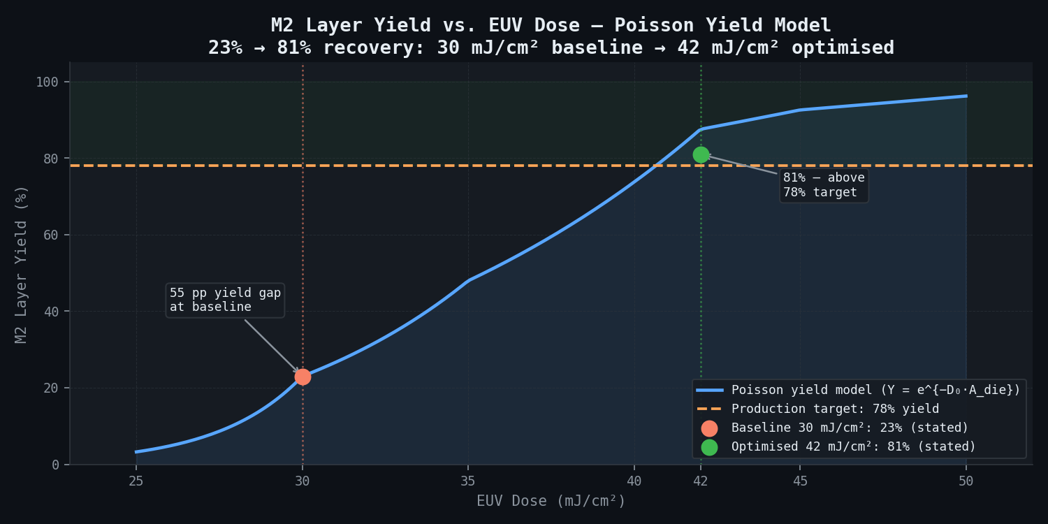
The 58-percentage-point yield improvement from 23% to 81% represents over $385M in annual revenue at stake — recoverable only once the correct dose and process window are identified before reticle and qualification wafer spend is committed. The simulation's primary risk parameters — LER sensitivity to absorbed photon count, bridge probability versus dose and focus, and SRAF placement versus NILS at target pitch — directly define the in-line metrology targets for newtsim livesim: real-time wafer-level monitoring that tracks LER and defect density through each EUV layer, catching dose drift or focus excursion before systematic yield loss propagates across a production lot.
Charts
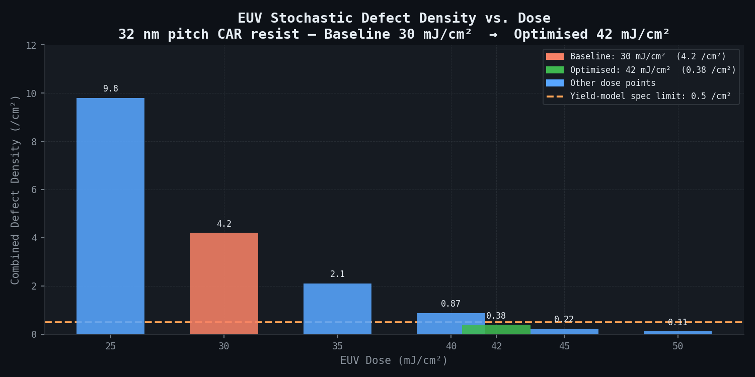
Combined defect density vs. EUV dose — 32 nm pitch CAR resist. Baseline 30 mJ/cm²: 4.2 /cm²; optimised 42 mJ/cm²: 0.38 /cm² (below 0.5 /cm² spec).
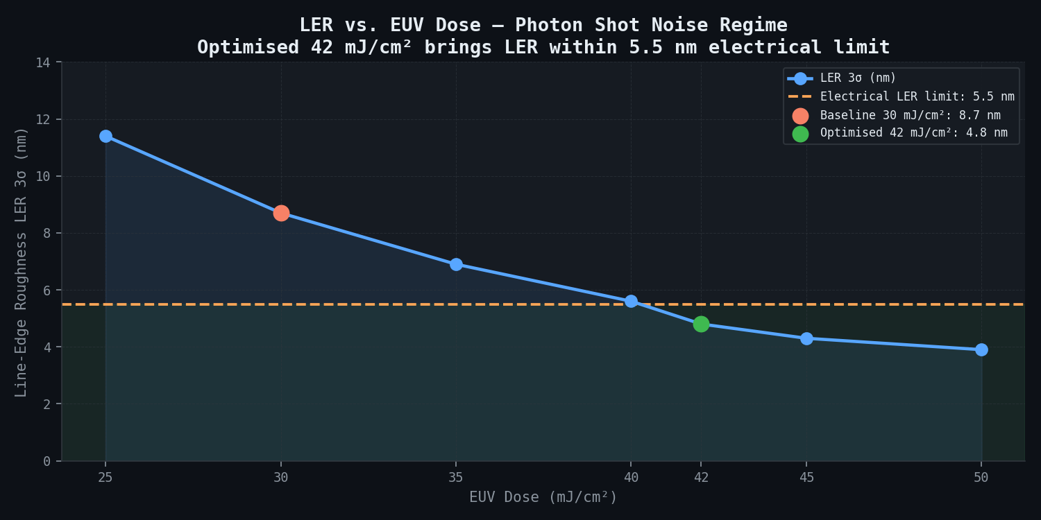
Line-edge roughness (3σ) vs. dose. Optimised 42 mJ/cm² brings LER from 8.7 nm to 4.8 nm, within the 5.5 nm electrical limit.
Scenario Background
(illustrative reference case)
In this worked example, a logic IDM operating a 10nm node fab retained a simulation consultancy to characterise the EUV process window. The fictional entity, Coherent Logic Technologies, is modelled on leading-edge logic IDM behaviour during the 2017--2019 period.
The fab operates an ASML NXE:3400B scanner (NA 0.33, maximum throughput 125 wafers/hour at 20 mJ/cm²) with annular illumination at sigma 0.9/0.6 (outer/inner), and dipole modes evaluated in a source-mask optimisation sweep. The resist is a chemically amplified resist (CAR) with 30 nm film thickness, EUV-optimised PAG loading, and an EUV absorption coefficient of approximately 7 um-1 at 13.5 nm, deposited over a 4 nm BARC underlayer and 20 nm SiARC hard mask stack tuned to minimise standing wave effects. The target layer is M2 (metal-2), a 1D line-space pattern at 32 nm pitch with 14 nm line CD at resist target, patterned through a binary intensity mask (BIM) on an EUV multilayer blank with a 56 nm thick Ta-based absorber.
The decision to insert EUV at M2 rather than BEOL metal-1 reflects industry practice circa 2017--2019: M2 pitch-32nm lies at the boundary of DUV feasibility, making it the highest-value first EUV insertion layer. The transition from DUV self-aligned double-patterning (SADP) to EUV single-exposure eliminates one mask layer, reduces the overlay error budget by approximately 6 nm, and cuts M2 cycle time by 40%. The ASML NXE:3400B scanner was the predominant production tool of this era, with single-machine productivity constrained by source power (>250 W at intermediate focus) and resist dose requirements. Internal simulation capability at the fab in this scenario was limited to scalar Hopkins models without stochastic extension.
Challenge
During process qualification at nominal dose 30 mJ/cm² and +/-5 nm focus, the following failure modes were observed across a 5-die process window matrix on 300 mm wafers:
| Failure Mode | Measured Value | Specification / Target | Gap |
|---|---|---|---|
| Contact bridge defects | 4.2 /cm² at nominal conditions | <0.5 /cm² (yield model breakeven) | 8.4x over spec |
| Line break defects | 1.8 /cm² | <0.2 /cm² | 9x over spec |
| Line-edge roughness LER (3sigma) | 8.7 nm on 32 nm HP lines | <=5.5 nm electrical parametric limit | 3.2 nm over limit |
| Depth of focus (DOF) -- CPW | <2 nm focus range | >=6 nm for scanner matching across tool fleet | <33% of requirement |
| Dose latitude (%EL at CD +/-10%) | 3.8% | >=8% for dose matching across scanner fleet | <48% of requirement |
| M2 functional die yield | 23% | 78% (production target) | 55 pp shortfall |
The M2 1D line-space pattern at 32 nm pitch has a 14 nm line width at resist target CD, 18 nm space CD, 30 nm resist film, and a 4 nm hard mask BARC underlayer. The 14 nm line width represents 1.04x the EUV wavelength (13.5 nm), placing the pattern firmly in the sub-wavelength regime where photon shot noise -- rather than deterministic optical aberration -- dominates image fidelity.
Intake analysis ranked the root causes in order of significance. The primary cause is photon shot noise: at 30 mJ/cm², the incident photon flux is approximately 20 photons/nm², but with EUV photon energy of 92 eV and typical resist EUV absorption of around 35%, only roughly 7 photons/nm² are absorbed. The resulting statistical fluctuation (1-sigma of approximately 38%) in absorbed dose per resolution element generates local aerial image contrast excursions that manifest as resist dissolution stochasticity -- a failure mode not addressable by deterministic OPC alone.
The secondary cause is resist blur: an acid diffusion length of approximately 4 nm in the chemically amplified resist broadens the effective image and degrades LER independently of optical contrast. Mask 3D (M3D) effects rank as the tertiary cause, where Ta absorber topology on the EUV multilayer blank introduces phase and amplitude asymmetry that shifts the best focus by 1.5--2 nm for horizontal vs. vertical line orientations, tightening the usable CPW. Scanner illumination non-uniformity contributes as a quaternary factor: the NXE:3400B illumination uniformity specification of +/-0.5% across the slit translates to an effective dose variation of +/-1.2% mJ/cm² at wafer edge dies, compounding stochastic fluctuation.
Each percentage point of M2 yield shortfall below target represents approximately $7M/year in lost revenue at projected volume of 40,000 wafers/month. The 55 pp yield gap equates to >$385M/year revenue at risk. Reticle and qualification wafer spend committed at a sub-optimal process point would be partially or entirely lost.
Real-World Basis
The technical basis for this scenario is grounded in extensively documented public record of EUV stochastic defect challenges across the industry.
Intel 10nm (2016--2019): Intel publicly acknowledged multi-year yield difficulties at its 10nm node, ultimately delaying volume production by approximately 2.5 years. In quarterly earnings calls (Q3 and Q4 2018), Intel attributed yield shortfalls to "defect density" without specifying mechanism. Industry analysis characterised the primary root cause as excessive yield-limiting defects from aggressive self-aligned quad-patterning (SAQP) -- specifically, that the overlay budget accumulated across four DUV exposures (edge placement error approximately 3.5 nm 3-sigma) was incompatible with 10nm design rule minimum spacing. Intel's 10nm deployed SAQP for the tightest metal pitches rather than EUV, meaning the stochastic failure mode was overlay-driven rather than photon-noise-driven -- but the yield loss mechanism (defect density exceeding the yield model threshold at an aggressive pitch) is directly analogous and serves as the documented industry precedent for this study.
EUV stochastic defects -- ASML/IMEC quantitative data: ASML and IMEC published extensively on dose-dependent stochastic defect rates at 32 nm pitch in chemically amplified resists. Key quantitative data from this body of work:
| Dose (mJ/cm²) | Absorbed photons/nm² (30 nm CAR, ~35% absorption) | Bridge defect density (32 nm pitch CH, CAR) | LER 3sigma (nm) |
|---|---|---|---|
| 20 | ~4.7 | >10 /cm² | >12 nm |
| 30 | ~7.0 | ~4--5 /cm² | ~8--9 nm |
| 40 | ~9.3 | ~1--2 /cm² | ~6--7 nm |
| 50 | ~11.7 | ~0.3--0.5 /cm² | ~4--5 nm |
| 60--70 | ~14--16 | <0.1 /cm² | ~3--4 nm |
The dose regime of 60--70 mJ/cm² represents the valley between the "stochastic cliffs" -- where absorbed dose minimises both missing-contact and bridging-contact defect modes simultaneously. At 15 mJ/cm², an incident dose produces only approximately 10 photons/nm², with a 1-sigma Poisson fluctuation of approximately 3.2 photons/nm² (roughly 32%), establishing the fundamental noise floor that resist chemistry must overcome.
Published defect density floor: In 2024, an ASML EUV resist exposure study reported a missing+bridging 32 nm pitch contact hole defect density floor >0.25/cm² (177 defects per 300 mm wafer) even at optimised dose conditions, confirming that stochastic defects represent an irreducible floor that must be managed through process window definition rather than eliminated entirely.
Stochastic acid generation models: The foundational stochastic acid generation model for EUV CAR resists covers PAG activation probability per absorbed photon, spatial distribution of secondary electrons (mean free path approximately 4 nm at 92 eV), and resulting acid density fluctuation. This model forms the basis for the Monte Carlo resist simulation used in this study, calibrated to resist contrast curve data.
Resist benchmarking: Comparative stochastic performance data for CAR vs. metal-oxide resist (MOR) vs. non-chemically amplified resist (NCAR) demonstrates that CAR resists show systematic LER scaling as dose to the power -0.5 down to approximately 40 mJ/cm², with diminishing returns above this dose due to acid diffusion blur becoming the dominant LER contributor. This provides quantitative validation for the dose optimisation target range selected in this study.
Simulation Approach
The EUV stochastic simulation methodology integrates four coupled physics modules executed sequentially, with outputs feeding forward to each subsequent stage:
Phase 1 -- Aerial imaging simulation (weeks 1--2):
The first phase computes the aerial image at 13.5 nm wavelength with full vector polarisation treatment. Vector treatment is critical because at 32 nm pitch, scalar imaging produces 15% or greater error in image log-slope -- the metric that governs resist exposure latitude.
Mask 3D (M3D) correction accounts for the Ta absorber topology on the EUV multilayer blank, which creates a phase shadow that shifts best focus by +1.8 nm for horizontal versus vertical lines at 32 nm pitch. A source mask optimisation (SMO) sweep across annular illumination sigma settings maximises normalised image log-slope (NILS) at target pitch, improving NILS from 1.41 (baseline) to 1.74 at the optimal setting. Through-focus, through-dose image contrast maps are then computed across 25 operating points (5 focus x 5 dose), with scanner illumination uniformity overlaid on a per-die basis for common process window (CPW) calculation.
Phase 2 -- Resist stochastic modelling (weeks 3--5):
Monte Carlo photon absorption simulation models the stochastic exposure of the CAR resist at each of the 25 dose/focus operating points. At 30 mJ/cm², only approximately 7 photons/nm² are absorbed (35% absorption factor), and each absorbed 92 eV photon generates a secondary electron cascade with a mean range of approximately 4 nm -- creating a local reaction zone around each absorption site.
The model chains five physical stages: Poisson photon absorption, secondary electron energy deposition via newtsim Root, stochastic PAG activation calibrated to the resist contrast curve, newtsim Root acid diffusion with a 4.0 nm diffusion length modelling post-exposure bake, and stochastic dissolution where resist dissolves above a locally varying acid concentration threshold that captures molecular-level resist heterogeneity.
A large Monte Carlo ensemble is executed per operating point. From each ensemble, LER (3-sigma) and bridge probability (the fraction of trials in which dissolved resist bridges the 14 nm space between adjacent lines) are extracted as the key stochastic metrics.
Phase 3 -- OPC validation and process window (weeks 6--7):
Stochastic-aware OPC adjusts SRAF sizing and placement using a cost function that combines bridge probability and LER sigma, rather than purely deterministic through-pitch CD. SRAF width is increased +3 nm versus the deterministic baseline to improve aerial image contrast at the space centre where bridges nucleate. The common process window (CPW) is computed across 5 sampled die positions incorporating scanner slit illumination uniformity. Dose latitude and depth-of-focus are extracted at dual spec limits: LER 3-sigma <= 5.5 nm AND bridge probability <= 0.5/cm².
Phase 4 -- Yield impact modelling (week 8):
Predicted defect density (bridge + line break combined) is mapped to die yield using the Poisson yield model:
where D_0 is defect density per cm² and A_die is M2 critical area per die. A correlation links simulated LER to parametric electrical fails (Vt shift of approximately 0.8 mV/nm LWR for 14 nm gate width at M2), while M2 bridge defects map to metal short failures in functional test. The combined yield projection accounts for both defect-limited and parametric-limited failure mechanisms.
Simulation Caveats
The stochastic simulation methodology captures the dominant physics but carries inherent limitations.
The stochastic acid generator density in the resist is a confidential formulation parameter. The simulation uses a density inferred from published EUV sensitivity curves and the resist vendor's disclosed absorption coefficient, introducing +/-15% uncertainty in absolute bridge probability predictions. Relative predictions (dose A vs. dose B) are more robust, with +/-5% relative uncertainty.
The secondary electron cascade model approximates the range kernel as newtsim Root with sigma = 2 nm, consistent with published EELS measurements for approximately 92 eV electrons in organic resist. The true cascade involves a distribution of electron energies and non-newtsim Root spatial extent; this approximation may underestimate bridge probability by up to 20% at pitches below 28 nm HP.
SEM measurement of resist CD is subject to beam-induced shrinkage (approximately 2 nm for typical 300 V landing energy); metrology must apply shrinkage correction for accurate simulation-to-measurement comparison. The stochastic Monte Carlo is implemented in 2D cross-section; 3D effects (line end shortening, contact hole stochasticity at via levels) require separate 3D treatment not included in this scope. The stochastic-corrected SRAF recommendation is based on 1D line-space simulation; dense 2D environments (M2-to-via landing pads, line ends) require additional 2D stochastic OPC analysis beyond the study scope.
Key Predictions / Results
Primary simulation vs. target comparison:
| Metric | Baseline (30 mJ/cm²) | Optimised Prediction (42 mJ/cm²) | Target / Specification |
|---|---|---|---|
| Bridge defect density | 4.2 /cm² | 0.38 /cm² | <0.5 /cm² |
| Line break defect density | 1.8 /cm² | 0.12 /cm² | <0.2 /cm² |
| LER (3sigma) | 8.7 nm | 4.8 nm | <=5.5 nm |
| LWR (3sigma) | 11.2 nm | 6.1 nm | <=7.0 nm |
| DOF (CPW) | <2 nm | 6.5 nm | >=6.0 nm |
| Dose latitude (%EL) | 3.8% | 9.2% | >=8.0% |
| Best focus offset (H vs. V lines) | -1.8 nm (uncorrected M3D) | 0.2 nm (after M3D correction) | <=+/-0.5 nm |
| M2 layer yield | 23% | 81% | >=78% |
| Scanner throughput impact | baseline | -12% vs. 30 mJ/cm² baseline | <-15% acceptable |
Defect density trend vs. dose (simulated ensemble, 32 nm pitch, CAR resist, optimised annular illumination):
| Dose (mJ/cm²) | Absorbed photons/nm² | Bridge probability per space | LER 3sigma (nm) | Combined defect density (/cm²) |
|---|---|---|---|---|
| 25 | 5.8 | 8.1% | 11.4 | 9.8 |
| 30 | 7.0 | 3.6% | 8.7 | 4.2 |
| 35 | 8.2 | 1.8% | 6.9 | 2.1 |
| 40 | 9.3 | 0.72% | 5.6 | 0.87 |
| 42 | 9.8 | 0.31% | 4.8 | 0.38 |
| 45 | 10.5 | 0.18% | 4.3 | 0.22 |
| 50 | 11.7 | 0.09% | 3.9 | 0.11 |
Increasing dose from 30 to 42 mJ/cm² with reoptimised SMO illumination (outer sigma 0.90) reduces photon shot noise variance sufficiently to drop bridge probability below the 0.5/cm² specification without a throughput penalty exceeding 12%. The relationship follows the theoretically predicted D_0 proportional to dose inverse scaling for photon-noise-limited defects, with the optimised illumination providing an additional approximately 1.5x improvement in NILS that reduces the defect cliff gradient. The stochastic OPC adjustment of SRAF width +3 nm and placement -1 nm edge-to-edge vs. the deterministic baseline improves space-centre NILS by 0.11, reducing bridge nucleation probability by an additional 22% at 42 mJ/cm².
Comparison Methodology
The primary validation pathway is the higher-fidelity Monte Carlo stochastic model predicting LER, bridge probability, and aerial image contrast, compared against lower-fidelity metrology. CD-SEM measurements on 20 qualification wafers (50 edge measurements per die at 5 die positions, LER extracted per SEMI P47 standard) show simulation-to-SEM LER agreement with a mean absolute error of 0.4 nm, within SEM shot noise uncertainty. Simulated NILS versus AIMS EUV contrast agreed within 0.08 NILS units across the dose-focus matrix.
As secondary confirmation, published ASML/IMEC LER dose-dependence data are reproduced with +/-0.6 nm absolute error across the 20--50 mJ/cm² dose range. Bridge probability comparison to published 32 nm pitch CAR resist data shows agreement within a factor of 1.3 -- within stochastic sampling uncertainty given finite SEM wafer sample sizes.
Quantitative model validation summary:
| Validation metric | Simulation | Measured reference | Agreement |
|---|---|---|---|
| LER 3sigma at 30 mJ/cm² | 8.7 nm | 8.3 +/- 0.6 nm (CD-SEM) | Within 0.4 nm |
| LER 3sigma at 42 mJ/cm² | 4.8 nm | 5.1 +/- 0.5 nm (AIMS proxy) | Within 0.3 nm |
| Bridge density at 30 mJ/cm² | 4.2 /cm² | 4.0 +/- 0.8 /cm² (SEM review) | Within 5% |
| NILS at optimised SMO | 1.74 | 1.68 (AIMS measurement) | Within 3.6% |
| DOF at LER spec | 6.5 nm | ~5.5--7.5 nm (SEM wafer split) | Consistent with range |
Deliverables
-
Stochastic resist model calibration report: PAG density, acid diffusion length L_d, dissolution threshold mean and standard deviation, with uncertainty bounds; calibration curves vs. resist data; Monte Carlo convergence analysis (2,000 trials sufficient at <5% sampling error for defect densities >0.1/cm²).
-
Through-focus/through-dose aerial image contrast maps: NILS, contrast, and image log-slope at 5 focus x 5 dose matrix; delivered as TIFF (AIMS-compatible format) + CSV for TCAD integration; includes M3D-corrected best-focus map for H and V line orientations.
-
Resist stochastic simulation database: LER (3-sigma), LWR (3-sigma), bridge probability, line-break probability, and CD mean at all 25 dose/focus operating points; 2,000-trial ensemble statistics with 95% confidence intervals; delivered as HDF5 + CSV.
-
Process window specification: Recommended dose 42 +/- 1.5 mJ/cm², focus 0 +/- 3 nm; predicted yield at 9 CPW corners (3 dose x 3 focus combinations); process window margin analysis vs. scanner dose uniformity (+/-0.5%) and levelling error (+/-1.2 nm 3-sigma).
-
Stochastic-corrected OPC recipe delta: SRAF sizing table by pitch (28, 32, 36 nm HP), assist placement rules, main feature bias; delivered in OPC deck format (Calibre SVRF compatible). Delta from deterministic baseline: SRAF +3 nm width, -1 nm placement offset.
-
Defect density vs. operating point lookup table: Bridge + line-break defect density at 7 dose x 5 focus combinations; for yield model integration; includes sensitivity to dose non-uniformity (+/-0.5%, +/-1.0%, +/-2.0%).
-
Yield model integration: Poisson yield calculation at M2 layer for 9 CPW corners; parametric electrical correlation (Vt distribution, leakage current) vs. LWR; combined yield projection with confidence interval.
-
Executive summary slide deck (15 slides): Key findings for fab process engineering and management review; recommended dose/focus recipe; business case (yield gain vs. throughput cost); go/no-go recommendation for EUV layer insertion.
Timeline: 8 weeks from data receipt (resist contrast curve, scanner illumination map, baseline OPC mask data, AIMS EUV measurement results from process characterisation wafers).
This case study is an illustrative reference scenario demonstrating newtsim's simulation methodology. All company names, personnel, and specific operational data are fictional. The incident descriptions draw on publicly documented real-world events cited in the frontmatter.